
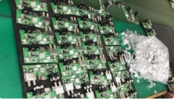
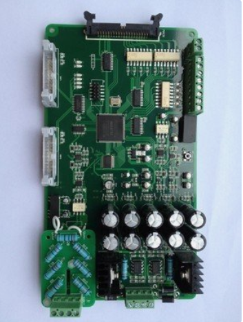
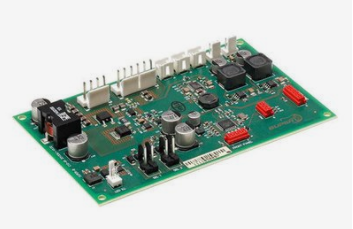
Professional PCB manufacturing and assembly
Building 6, Zone 3, Yuekang Road,Bao'an District, Shenzhen, China
+86-13410863085Mon.-Sat.08:00-20:00

(1) Check the user's PCB file
The PCB files brought by users should be checked routinely first:
1. Check whether the disk file is intact;
2. Check whether the file contains a virus. If there is a virus, you must kill it first;
3. If it is a Gerber file, check whether there is a D code table or whether it contains a D code.
(2) Check whether the design conforms to the process level of PCB factory
1. Check whether the various distances designed in the customer file conform to the PCB factory process: the distance between lines, the distance between lines and pads, and the distance between pads. The above distances shall be greater than the minimum distance that can be reached by the production process of PCB factory.

2. Check the width of the wire. It is required that the width of the wire should be greater than the minimum that can be achieved by the production process of the PCB factory
Lineweight.
3. Check the size of the through hole to ensure the minimum hole diameter of the PCB factory's production process.
4. Check the size of PCB pad and its internal hole diameter to ensure that the pad edge has a certain width after PCB drilling.
(3) Determine PCB process requirements
Determine various process parameters according to user requirements.
PCB process requirements:
1. Determine whether the photo negative (commonly known as film) is mirrored according to different requirements of the subsequent process. The principle of negative image: the drug film surface (i.e., emulsion surface) is pasted on the drug film surface to reduce the error. The decisive factor of negative image: process. In case of screen printing process or dry film process, the film surface of the negative film shall be pasted on the copper surface of the substrate. If the diazo film is used for exposure, the mirror image of the diazo film shall be that the film surface of the negative film does not stick to the copper surface of the substrate. If the photo is a unit negative rather than a photo plate, an additional mirror image is required.
2. Determine the parameters of resistance welding expansion.
Determination principle:
① The wire next to the PCB pad must not be exposed.
② Small cannot cover the pad.
Due to the error during operation, the resistance welding diagram may deviate from the line. If the solder resistance is too small, the deviation may cause the pad edge to be covered. Therefore, the resistance welding shall be larger. However, if the resistance welding expands too much, the nearby wires may be exposed due to the influence of deviation.
It can be seen from the above requirements that the decisive factors for the expansion of resistance welding are:
① Deviation value of PCB factory resistance welding process position and resistance welding figure.
Because the deviation caused by various PCB processes is different, the solder resistance amplification value corresponding to various processes is also
Different. The expanded value of resistance welding with large deviation shall be larger.
② The board wire density is large, the space between the pad and the wire is small, and the solder resistance expansion value should be smaller; plate
The sub conductor density is small, and the resistance welding amplification value can be larger.
3. According to whether there is a printed plug (commonly known as golden finger) on the board, determine whether to process the art line.
4. Determine whether to add conductive frame for electroplating according to electroplating process requirements.
5. Determine whether to add conductive process line according to the requirements of hot air leveling (commonly known as tin spraying) process.
6. Determine whether to add the center hole of the pad according to the drilling process.
7. Determine whether to add process positioning holes according to the subsequent process.
8. Determine whether to add outline corner lines according to the board shape.
9. When the user requires high line width accuracy for high-precision boards, determine whether to correct the line width according to the production level of the factory to adjust the impact of side erosion.
(4) CAD files converting to Gerber files
In order to carry out unified management in CAM process, all CAD files should be converted to standard format Gerber of photo plotter and equivalent D code table.
In the conversion process, attention should be paid to the required process parameters, because some requirements are to be completed in the conversion.
Now, in addition to Smart Work and Tango software, all common CAD software can be converted to Gerber. The above two software can also be converted to Protel format and then Gerber through tool software
(5) CAM Processing
Carry out various process treatment according to the determined process.
Special attention shall be paid to: whether there are any places in the user file with too small spacing, which must be handled accordingly
(6)PCB photo drawing (CAM)
The files processed by CAM can be photographed and output to PCB.
The composition can be carried out in CAM or output.
A good photo system has certain CAM functions, and some process processing must be carried out on the photo machine, such as line width correction.
(7) Darkroom treatment
The photographic negative of PCB circuit board needs to be developed and fixed before it can be used in subsequent processes. During darkroom treatment, the following links shall be strictly controlled:
Developing time: it affects the optical density (commonly known as blackness) and contrast of the production plate. Short time, insufficient optical density and contrast; If the time is too long, the fog will increase.
Fixing time: If the fixing time is not enough, the background color of the production plate is not transparent enough.
Non washing time: if the washing time is not enough, the production plate will turn yellow.
Special attention: Do not scratch the film.


Just upload Gerber files, BOM files and design files, and the KINGFORD team will provide a complete quotation within 24h.