
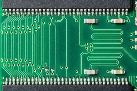
Professional PCB manufacturing and assembly
Building 6, Zone 3, Yuekang Road,Bao'an District, Shenzhen, China
+86-13410863085Mon.-Sat.08:00-20:00

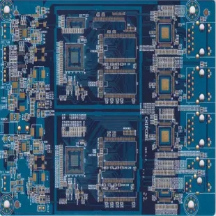
Detailed explanation of PCB process chip packaging technology
1. BGA (ball grid array) is also called CPAC (global top pad array carrier). Spherical contact arrangement, one of surface mount packages. A spherical bump is made on the back of the printed substrate in the display mode to replace the pin, LSI chips are assembled on the front of the printed substrate, and then sealed with molding resin or potting method. Also known as a bump display carrier (PAC). The pins can exceed 200, which is a package used for multi pin LSI. The package body can also be smaller than QFP (four side pin flatpack). For example, the 360 pin BGA with a pin center distance of 1.5mm is only 31mm square; The QFP of 304 pin with 0.5mm center distance is 40mm square. And BGA doesn't have to worry about pin deformation like QFP.
The package was developed by Motorola Company in the United States. It was first used in portable phones and other devices, and then popularized in personal computers. Initially, the center distance of BGA pins (bumps) is 1.5mm, and the number of pins is 225. Now some LSI manufacturers are developing 500 pin BGA. The problem with BGA is the appearance inspection after reflow. Motorola of the United States calls the package sealed with molded resin OMPAC, and the package sealed by potting method GPAC.
2. C - (ceramic) indicates the mark of ceramic package. For example, CDIP represents ceramic DIP. It is a mark often used in practice.
3. COB (chip on board) chip packaging is one of the bare chip mounting technologies. Semiconductor chips are connected and mounted on the printed circuit board. The electrical connection between the chip and the substrate is realized by wire stitching and covered with resin to ensure reliability. Although COB is the simplest bare chip mounting technology, its package density is far less than TAB and flip chip bonding technology.
4、DIP(dual in-line package)
Dual in-line package. One of the plug-in packages, the pins are led out from both sides of the package, and the packaging materials are plastic and ceramic. DIL is widely used by European semiconductor manufacturers.
DIP is the most popular plug-in package, and its application range includes standard logic IC, memory LSI, microcomputer circuit, etc. The pin center distance is 2.54mm, and the number of pins is from 6 to 64. The package width is usually 15.2mm. Some packages with a width of 7.52mm and 10.16mm are called SK DIP (skinny dual in line package) and SL DIP (slim dual in line package) narrow DIP respectively. However, in most cases, it is not differentiated and is simply referred to as DIP. In addition, ceramic DIPs sealed with low melting point glass are also called Cerdip (see 4.2).
4.1 Alternative name for DIC (dual in line ceramic package) ceramic package (including glass seal).
4.2 Cerdip: glass sealed ceramic dual in-line package, used for ECL RAM, DSP (digital signal processor) and other circuits. Cerdip with glass window is used for ultraviolet erasable EPROM and microcomputer circuit with EPROM inside. The center distance of pins is 2.54mm, and the number of pins ranges from 8 to 42. In Japan, this package is referred to as DIP-G (G means glass seal).
4.3 SDIP (shrink dual in line package) shrink type DIP. It is one of plug-in packages with the same shape as DIP, but the pin center distance (1.778mm) is less than DIP (2.54mm). The number of pins ranges from 14 to 90. There are two kinds of ceramics and plastics. Also known as SH - DIP (shrink dual in line package)
5、flip-chip
Backweld the chip. As one of the bare chip packaging technologies, the metal bump is made in the electrode area of LSI chip, and then the metal bump is pressure welded with the electrode area on the printed substrate. The footprint of the package is basically the same as the chip size. It is the smallest and thinnest of all packaging technologies. However, if the thermal expansion coefficient of the substrate is different from that of the LSI chip, it will react at the junction, thus affecting the reliability of the connection. Therefore, resin must be used to reinforce LSI chips, and substrate materials with basically the same thermal expansion coefficient must be used.
6、FP(flat package)
Flatpack. One of the surface mount packages. Alternative name for QFP or SOP (see QFP and SOP). Some semiconductor manufacturers use this name.
7、H-(with heat sink)
Indicates a mark with a radiator. For example, HSOP stands for SOP with radiator.
8、MCM(multi-chip module)
Multichip module. A package that assembles multiple semiconductor bare chips on a wiring substrate. According to the substrate materials, it can be divided into three categories: MCM-L, MCM-C and MCM-D. MCM-L is a component that uses a common glass epoxy multilayer printed substrate. The wiring density is not very high and the cost is low. MCM-C is a component that uses thick film technology to form multilayer wiring, and uses ceramics (aluminum oxide or glass ceramics) as the base plate. It is similar to thick film hybrid ICs that use multilayer ceramic substrates. There is no significant difference between the two. The wiring density is higher than MCM-L. MCM-D is a module that uses thin film technology to form multilayer wiring and takes ceramics (aluminum oxide or aluminum nitride) or Si, Al as the substrate. Cabling conspiracy is the highest among the three components, but the cost is also high.


Just upload Gerber files, BOM files and design files, and the KINGFORD team will provide a complete quotation within 24h.