
Professional PCB manufacturing and assembly
Building 6, Zone 3, Yuekang Road,Bao'an District, Shenzhen, China
+86-13410863085Mon.-Sat.08:00-20:00

1. PCB VS FPC
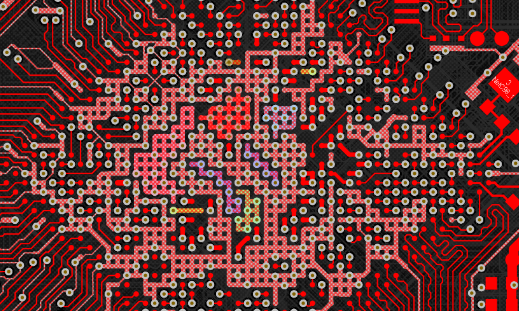
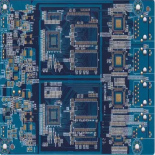
PCB is one of the important electronic components in the electronic industry. Almost every kind of electronic equipment, such as electronic watches, calculators, computers, communication electronic equipment, military weapon systems, etc., as long as there are integrated circuits and other electronic components, need to use printed boards for electrical interconnection. PCB has developed from single-sided to double-sided, multi-layer and flexible, and has been developing towards high-precision, high-density and high reliability, and continuously reducing the size, reducing costs, and improving performance, so that PCB has always maintained strong vitality in the development of electronic equipment.
Compared with the hard circuit board, the soft board of the flexible circuit board is flexible, and has the advantages of easy turning, light weight, thin thickness, etc. The soft board product structure is made of the soft copper foil substrate and the soft insulation layer, which are pressed together after adhesive (glue) bonding, and has many advantages that the hard printed circuit board does not have. For example, free bending, winding and folding can be arranged arbitrarily according to the space layout requirements, and can be moved and expanded arbitrarily in three-dimensional space, so as to achieve the integration of element, piece assembly and wire connection. The flexible circuit board can greatly reduce the volume of electronic products, which is suitable for the development of electronic products in the direction of high density, miniaturization and high reliability. Therefore, FPCB has been widely used in aerospace, military, mobile communications, laptops, computer peripherals, PDAs, digital cameras and other fields or products.
FPC production
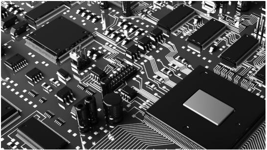
PCB and FPC are important components and line connection carriers in 3C industry.
With the continuous development of intelligence in the electronic industry, PCBs are becoming smaller and thinner, which contain more and more PCB components and require higher and higher machining precision. At the same time, the application of laser on PCB and flexible circuit board is more and more extensive!
2. Application of laser in PCB and FPC manufacturing
With the development of flexible circuits, smaller and more complex flexible circuit boards will become the development direction in the future. The traditional processing method is difficult to meet the processing needs due to its own conditions. In order to achieve more refined flexible circuit design, more refined processing solutions are needed
1. Laser marking
Laser marking has high precision, fast speed and stable performance. It only needs to be controlled by a computer. It is easy to operate. It can print all kinds of complex patterns, characters, two-dimensional codes and other contents. It is non-contact processing, non consumable, environmentally friendly and pollution-free. It fully meets the requirements of the existing PCB and flexible circuit board industry for high-quality marking. It can make up for the lack of silk screen processing, and gradually becomes the best processing tool for PCB marking, playing a pivotal role in the circuit board industry!
Ultraviolet laser marking machine, with high-energy laser beam, can convert light energy into chemical energy when acting on polymer materials such as PI. Under the action of precision laser beam, some chemical bonds connecting atoms and molecules of substances change, so as to achieve the purpose of surface treatment. In the process of processing, due to the processing time period and energy concentration, the surface of the processed articles will hardly be damaged. Therefore, both the machining accuracy and quality can be effectively guaranteed. Although the current UV laser marking machine is more expensive than traditional processing equipment, the PCB process requirements for marking are difficult to reach by other processing methods. In the future, laser technology will provide a more refined processing solution for flexible processing, and provide a strong guarantee for smaller and more complex flexible circuits in the future.
Compared with traditional printed PCB technology, laser marking technology has many advantages:
1) Good quality and strong wear resistance. The PCB board surface can be marked clearly and beautifully, and can be marked with various LOGOs, patterns, two-dimensional codes, and characters. The patterns are directly carved on the materials, so the wear resistance is more prominent;
2) High machining accuracy. The laser beam emitted by the laser can reach the minimum spot diameter of 10um (UV laser) after being focused, which is of great help in processing complex graphics and precision machining;
3) High efficiency, simple operation and low cost. Users only need to set the parameters on the computer to directly mark the material surface in a few seconds to more than ten seconds;
4) Non destructive marking. The laser marking adopts non-contact processing, and the laser head does not need to contact the material surface, so the damage to the material does not need to be considered;
5) Wide range of use, safety and environmental protection. Various thin metal/non-metallic materials can be marked;
6) Stable performance and long service life. With the development of PCB technology, the service life of lasers and equipment has been greatly extended.
2. Laser cutting
1) High precision
Compared with traditional cutting technology, laser cutting has a high precision. In general, taking the Han's Super Power MPS-0606LP model as an example, the positioning accuracy of laser cutting is ± 0.01mm, and the repeated positioning accuracy is 0.005mm. It is applicable to the cutting of precision accessories and fine cutting of various craft words and paintings.
2) Narrow slit
The laser beam is focused into a very small light spot, which makes the focus reach a very high power density. The material is quickly heated to the extent of gasification and evaporates to form holes. With the relative linear movement of the light beam and the material, the hole continuously forms a very narrow slit. The kerf width is generally 0.10-0.20mm. Compared with the traditional cutting technology, the kerf formed by laser cutting is very narrow.
3) Smooth cutting surface
Generally speaking, for some PCB industries or products with very high cutting requirements, no burrs are allowed. The traditional cutting technology can not meet this requirement, while the laser cutting technology can achieve the cutting surface without burrs.
4) Fast
Another significant advantage of the new laser cutting technology is that the cutting speed is very fast. Under normal circumstances, taking the Han's Super Power MPS-0606LP model as an example, the maximum acceleration can reach 1.5G, and the maximum positioning speed can reach 60m/min, which is much faster than the gongs and presses. For some demanding fields, laser cutting applications are also very frequent.
5) Good quality, no damage
Laser cutting belongs to non-contact cutting, and the cutting edge is little affected by heat. There is basically no thermal deformation of the workpiece, completely avoiding the collapse of the edge formed during material punching and shearing. Generally, the cutting seam does not need secondary processing. The laser cutting head will not contact the material surface to ensure that the workpiece will not be scratched.
6) Not affected by material properties
Laser can process steel plate, stainless steel, aluminum alloy plate, hard alloy and PCB industry substrates of various materials. No matter what the hardness, it can perform deformation free cutting. Laser processing is flexible and can be used to process arbitrary figures, as well as to cut pipes and other profiled materials.
7) Save mold investment Compared with punch processing, laser processing does not require mold, no mold consumption, no mold repair, save mold replacement time, thus saving processing costs, reducing production costs, especially suitable for processing large products.
8) Material saving
With computer programming, products of different shapes can be cut to maximize the utilization of materials.
9) Improve sample delivery speed.
After the product drawings are formed, laser processing can be carried out immediately to obtain the physical objects of new products in the shortest time.
10) Safety and environmental protection
High equipment integration, small floor area, less processing waste, low noise, clean, safe, pollution-free, greatly improving the working environment.
3. Advantages of green light/ultraviolet PCB laser cutting machine in processing PCB circuit boards
1) Compared with CO2 laser, the applicable materials are more extensive. In addition to aluminum substrate, almost all material products can be processed, such as FR4, fiberglass board, paper substrate, copper clad plate, etc. In addition, the wavelength of ultraviolet light and green light is shorter, the pulse width is small, the thermal effect is small, and there is no burning phenomenon.
2) The non-contact processing can be applied to any graphic processing without being affected. Therefore, compared with the traditional processing method, it does not need to make any adjustment in the PCB circuit board industry, and can effectively improve the response speed for any curve processing.
3. The processing effect is good, the laser wavelength is short, the thermal effect is small, the cutting edge is smooth, without burrs, and there will be no dust during the processing. It will not produce any stress on PCB circuit board and will not deform the board.
4) High cutting accuracy, camera positioning, cutting gap less than 50 microns, high cutting position accuracy. It is especially suitable for certain PCB sub board industries with high processing requirements.
5) The operation process is simple, the software is automatically controlled, and the automatic loading and unloading mechanism can be connected to save labor costs.


Just upload Gerber files, BOM files and design files, and the KINGFORD team will provide a complete quotation within 24h.