
Professional PCB manufacturing and assembly
Building 6, Zone 3, Yuekang Road,Bao'an District, Shenzhen, China
+86-13410863085Mon.-Sat.08:00-20:00

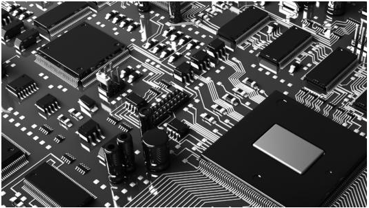
On the printed circuit board, copper is used to interconnect the components on the substrate. Although it is a good conductor material to form the conductive path of the printed circuit board, if it is exposed to the air for a long time, it is also easy to lose its luster due to oxidation
On the printed circuit board, copper is used to interconnect the components on the substrate. Although it is a good conductor material to form the conductive path of the printed circuit board, if it is exposed to the air for a long time, it is also easy to lose its luster due to oxidation, and lose its weldability due to corrosion. Therefore, various technologies must be used to protect copper printed wires, through holes and plated through holes, including organic painting, oxide film and electroplating technologies.
Organic paint is very simple to apply, but it is not suitable for long-term use due to changes in its concentration, composition and curing cycle. It may even lead to unpredictable deviation in weldability. The oxide film can protect the circuit from corrosion, but it cannot maintain solderability. Plating or metal coating process is a standard operation to ensure solderability and protect circuits from corrosion, and plays an important role in the manufacture of single-sided, double-sided and multi-layer printed circuit boards. In particular, plating a layer of solderable metal on the printed wire has become a standard operation to provide a solderable protective layer for copper printed wire.
The interconnection of various modules in PCB equipment often requires the use of a printed circuit board plug socket with spring contacts and a printed circuit board with connection contacts designed to match it. These contacts should have high wear resistance and low contact resistance, which requires a layer of rare metals, among which gold is the most commonly used metal. In addition, other coated metals can also be used on the printed line, such as tin plating, copper plating, and sometimes copper plating can be used in some areas of the printed line.
Another coating on the copper printing line is organic matter, usually a solder mask, which is coated with a layer of epoxy resin film using screen printing technology where welding is not required. This process with a layer of organic flux does not require electronic exchange. When the circuit board is immersed in the chemical plating solution, a compound with nitrogen resistance can stand on the exposed metal surface and will not be absorbed by the substrate.
The precise technology required by PCB products and the strict requirements of environmental and safety adaptability have promoted the electroplating practice to make great progress, which is obviously reflected in the technology of manufacturing multi substrate with high complexity and high resolution. In electroplating, through the development of automatic and computer controlled electroplating equipment, the development of highly complex instrument technology for chemical analysis of organic and metal additives, and the emergence of technology for precise control of chemical reaction process, electroplating technology has reached a very high level.
There are two standard methods to make metal layers grow in circuit board wires and through holes: circuit electroplating and full board copper plating, which are described as follows.
1. Line electroplating
In this PCB process, copper layer generation and etching inhibitor metal electroplating are only accepted where circuit patterns and through holes are designed. In the process of line electroplating, the increased width of each side of the line and welding pad is roughly equivalent to the increased thickness of the electroplating surface. Therefore, a margin needs to be left on the original negative.
In PCB circuit electroplating, most copper surfaces are basically shielded by an inhibitor, and electroplating is only carried out in places with circuit patterns such as lines and solder pads. As the surface area to be plated is reduced, the required power supply current capacity is usually greatly reduced. In addition, when contrast reversal photosensitive polymer dry film plating inhibitors (the most commonly used type) are used, their negative negative films can be made with relatively cheap laser printers or drawing pens. The anode consumes less copper in line electroplating, and the copper to be removed in the etching process is also less, thus reducing the analysis and maintenance costs of the electrolytic cell. The disadvantage of this technology is that the circuit pattern needs to be coated with tin/lead or a kind of electrophoretic inhibitor material before etching, which can be removed before welding inhibitor is applied. This increases the complexity and adds an additional set of wet chemical solution treatment process.
2. PCB full board copper plating
In this process, all surface areas and drilling holes are plated with copper, some inhibitor is poured on the unnecessary copper surface, and then the etching inhibitor metal is plated. Even for a medium size printed circuit board, it also requires an electric digger that can provide considerable current to make a smooth and bright copper surface that is easy to clean for subsequent processes. If there is no photoelectric plotter, you need to use a negative negative to expose the circuit graphics, making it a more common contrast inversion dry film photoresist. Etch the full board copper plated circuit board, and most of the PCB materials plated on the circuit board will be removed again
With the increase of medium copper carrier solution, the burden of additional corrosion on the anode is greatly increased.


Just upload Gerber files, BOM files and design files, and the KINGFORD team will provide a complete quotation within 24h.