
Professional PCB manufacturing and assembly
Building 6, Zone 3, Yuekang Road,Bao'an District, Shenzhen, China
+86-13410863085Mon.-Sat.08:00-20:00

With the social progress and the development of science and technology, emerging electronic products continue to emerge, expanding the application field and market of PCB products. At the same time, the demand for electronic information processing of various products is also gradually increasing. When the demand of the terminal market becomes personalized, diversified and customized, if the circuit board PCB wants to achieve a satisfactory performance, it must expand the board layer to more than two layers, so there is a multilayer PCB circuit board.
It is mainly the "core main force" in communication, medical treatment, industrial control, security, automobile, electric power, aviation, military industry, computer peripheral and other fields. According to the data released by Prismark, multilayer boards and flexible boards will still dominate in 2020, accounting for 37.39% and 20.01% respectively.
As the product functions become higher and higher, and the PCB becomes more and more precise, the production becomes more and more difficult. Compared with the characteristics of conventional circuit boards, high layer circuit boards have the characteristics of thicker boards, more layers, denser lines and vias, larger unit sizes, thinner dielectric layers, etc. The requirements for inner layer space, inter layer alignment, impedance control and reliability are stricter. In the face of the current PCB industry environmental protection, expensive labor, shrinking profits, fierce market competition and other issues, multi-layer circuit boards, because the cost is much higher than single and double-layer boards, coupled with the difficulty of quality control, if customers do not have the intention to order in large quantities, generally PCB manufacturers will find a substitute factory or put forward corresponding cooperation conditions, considering the cost still has cooperation value.
Moreover, many customers lack understanding of the process and have suffered a lot. Many PCB manufacturers fought a price war and once cut the price of single and double board proofing to an amazing single digit, even free. However, there is no advanced equipment in itself. In order to save costs, we can only find other manufacturers to do it. The key is that the manufacturers we find also have many defects. They are unqualified in equipment and technology, leading to uncontrollable quality. Finally, they are delivered to customers as inferior products, which can not give full play to the product performance.
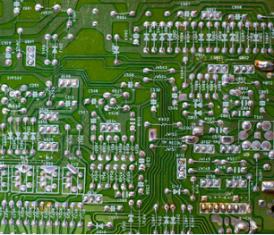
PCB multilayer board proofing
The quality, reliability and stability that customers have always cared about are also what Creator Factory has always attached importance to. As the number of PCB layers is more, the wiring difficulty index is also increased, so the requirements for manufacturing cost and process technology capability are relatively high. The Creator Factory has invested a lot of money and manpower in the research and development, management system, quality process control and other aspects of high multilayer boards, has mature manufacturing process capabilities and advanced process equipment, and has a team of professional PCB technicians and independent research and development engineers to meet the needs of customers for high multilayer boards and ensure the output and reliability of PCB product quality.
The advantages of our PCB circuit for the high multilayer boards required by the market are as follows:
1. 64 layers at most;
2. Backdrilling can reduce the loss of signal transmission;
3. Aperture ratio 15:1, plate thickness 0.4-10.0mm;
4. Blind hole technology, impedance control;
5. Reliable PCB technology is adopted, and the alignment deviation between layers can be controlled within 35um;
6. Adopt a special design method - ventilation hole design to improve the binding force between the copper layer and the hole wall.
7. In addition, our inner layer connection quality control method can improve PCB process parameters and special parameters, thereby improving the inner layer connection quality.
Probe into the Effect of Electroplating on PCB
Oct 30,2022


Just upload Gerber files, BOM files and design files, and the KINGFORD team will provide a complete quotation within 24h.