
Professional PCB manufacturing and assembly
Building 6, Zone 3, Yuekang Road,Bao'an District, Shenzhen, China
+86-13410863085Mon.-Sat.08:00-20:00

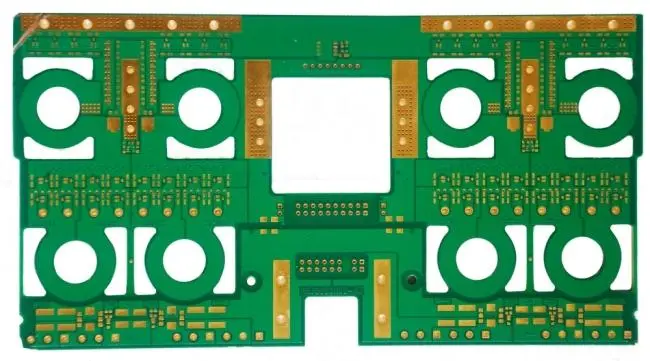
Nowadays, many circuit boards in electronic products use SMT manufacturing process, that is, surface mount technology, that is, all electronic components are soldered on the surface of circuit boards. It is not necessary to insert it from the reserved via on the circuit board and then weld it from the back as before.
SMT technology can make the production process of PCB more automatic and rapid, and reduce human intervention. In addition, the components used in this technology have the advantages of smaller volume, thinner and more reliable than the previous plug-ins.
A SMT production line includes the following main parts: printing machine, mounting machine, reflow furnace, cooling equipment and some auxiliary optical detection equipment, cleaning equipment, drying equipment and material storage equipment.
Now let's take a look at how a piece of adopted circuit board is produced.
First, according to the electronic material list of the circuit board, prepare the electronic components to be used and install them on the mounter. The installation method is to install the materials on the feeder, and then insert the feeder into the corresponding area of the mounter. What material number is placed in what area is fixed, which has been set by the technicians when writing the program before production. The prepared materials are waiting for the boards flowing down the assembly line.
We call this kind of circuit board without parts PCB. PCB needs to be manually pasted on a pallet one by one by an employee. How many PCB boards are placed on each pallet needs to be determined according to the size of the board.
The pallet for loading PCB boards is made of a high temperature resistant material. This board will load the entire process of PCB production, and then the staff at the end of the assembly line will take down the PCB boards with the parts installed. The empty pallet will return to the line head.
The first battle of the production line is to tin these PCB boards. It is to cover the steel mesh on the upper side of these boards. There are small holes on the steel mesh. These holes are facing the place where components need to be installed on the PCB board. This place is the bonding pad. The solder joints between components and PCB are controlled by the machine and uniformly brushed through the entire steel mesh. At this time, the PCB bonding pad position will be covered with solder paste with the thickness of the steel mesh.
The whole pallet will be loaded with printed tin PCBs, which will flow to the next station through the transmission track, and then the long waiting SMT station will be here. The components have been installed in the machine. At this time, the machine will install the components on the designated position of the PCB according to the program prepared by the technician in advance. The installation process is actually like taking a feeder and sucking the electronic materials one by one from the feeder, Put it on the PCB. Of course, the absorption speed is innumerable times that of human beings, and the error will not exceed one twentieth of the size of the element.
PCB with electronic components installed, waiting to flow to the next station
After the mounter has installed all the electronic parts, the carrier board will carry these PCBs loaded with the elements and flow into the last station in the manufacturing process, the high-temperature reflow furnace. The temperature in this furnace is enough to melt the solder paste, and the melted tin will firmly weld the components and PCBs together.
At the entrance of the reflow furnace, the PCB with components will be sent into the furnace through the rail
The boards flowing out of the reflow furnace have a high temperature. They need to be cooled by a cooling device before they can flow to the final optical detection station. At the end of this station, the manufacturing process of electronic circuit boards is basically completed. The next step is to detect the fabricated circuit boards.
After cooling, the carrier plate carries the fabricated PCB into the optical detection equipment for optical detection to confirm whether the components and PCB are well welded and whether there are defective products.
After the inspection of the optical testing equipment, the final visual inspection will be carried out by the personnel, and the welding condition of the circuit board will be finally confirmed with the electronic magnifying glass
Finally, the staff at the end of the line will take the checked circuit board off the pallet and put it into the special plastic pallet. The whole production process is completed.
All.


Just upload Gerber files, BOM files and design files, and the KINGFORD team will provide a complete quotation within 24h.