
Professional PCB manufacturing and assembly
Building 6, Zone 3, Yuekang Road,Bao'an District, Shenzhen, China
+86-13410863085Mon.-Sat.08:00-20:00

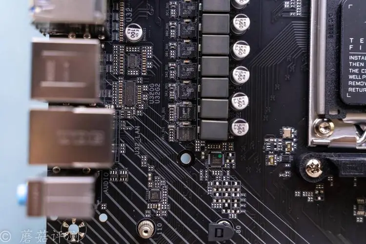
At present, the mass produced pcb hardware is manufactured using the well-known surface mount technology or SMT. There is no reason! In addition to providing many other advantages, SMT mobile phone wireless charging circuit board S still has a long way to go in accelerating the wireless charging speed of mobile phones.
SMT technology
Surface mount technology
In essence, surface mount technology (SMT) has adopted the basic concept of through-hole manufacturing and continues to make significant improvements. When using SMT, the mobile phone wireless charging circuit board does not need to be drilled. Instead, they use solder paste. In addition to increasing speed, this significantly simplifies the process. Although SMT mounting components do not have the strength of through hole mounting components, they offer many other advantages that can offset this problem.
Surface mount technology goes through the following five steps:
1. Production of mobile phone wireless charging circuit board - this is the stage of actually using SMT solder points to produce mobile phone wireless charging circuit board
2. Deposit solder on the pad to fix the assembly to the plate
3. With the help of the machine, place the components on the precise solder joints
4. Bake the wireless charging circuit board of mobile phone to harden the flux
5. Check the completed components
Reasons that make SMT different from through-hole include:
Through the use of surface mount technology, the space problem that widely occurs in through-hole installation can be solved. SMT also provides design flexibility because it gives mobile phone wireless charger board designers free control to create dedicated circuits. The reduced component size means that more components can be accommodated on one board, and fewer boards are required.
The components in the SMT installation are lead-free. Shorter lead lengths for surface mount components reduce propagation delays and package noise.
The density of components per unit area is higher because it allows the components to be mounted on both sides.
It is suitable for mass production, thus reducing the cost.
The reduction in size results in an increase in circuit speed. In fact, this is one of the main reasons why most manufacturers choose this method.
The surface tension of the molten solder pulls the assembly into alignment with the pad. This, in turn, automatically corrects any minor errors that may occur in component placement.
It has been proved that SMT is more stable in the presence of many vibrations or wobbles.
SMT parts are generally cheaper than similar through-hole parts.
Importantly, SMT can greatly reduce production time because no drilling is required. Moreover, SMT components can be placed thousands of times per hour, while the placement speed of through-hole installation is less than 1000 times. In turn, this led to the expected speed of product production, which further shortened the time to market. Therefore, if you want to speed up the production time of mobile phone wireless charging circuit board, SMT is undoubtedly the answer. By using DFM software tools, the need for rework and redesign of complex circuits can be greatly reduced, thus further improving the speed and the possibility of complex design.
All this does not mean that SMT has no inherent shortcomings. The SMT may not be reliable if it is used as the only method of securing components that face significant mechanical stresses. Components that generate a lot of heat or are subject to high electrical loads cannot be installed with SMT. This is because the solder will melt at high temperatures. Therefore, in case of failure of SMT due to special mechanical, electrical and thermal factors, it is likely to continue to use through hole installation. Similarly, SMT is not suitable for prototyping, because components may need to be added or replaced during prototyping, and high-density circuit boards may be difficult to support.


Just upload Gerber files, BOM files and design files, and the KINGFORD team will provide a complete quotation within 24h.