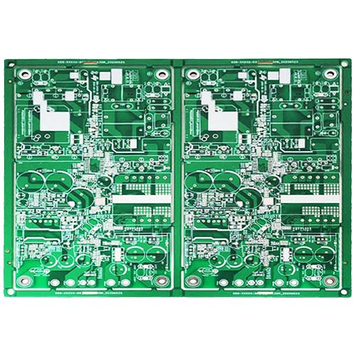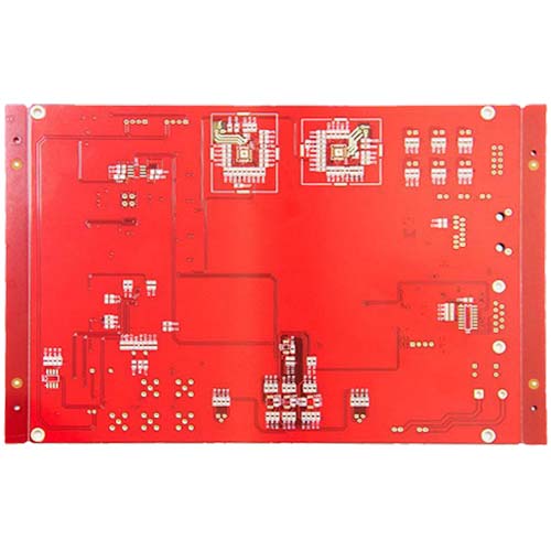
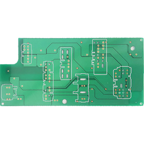
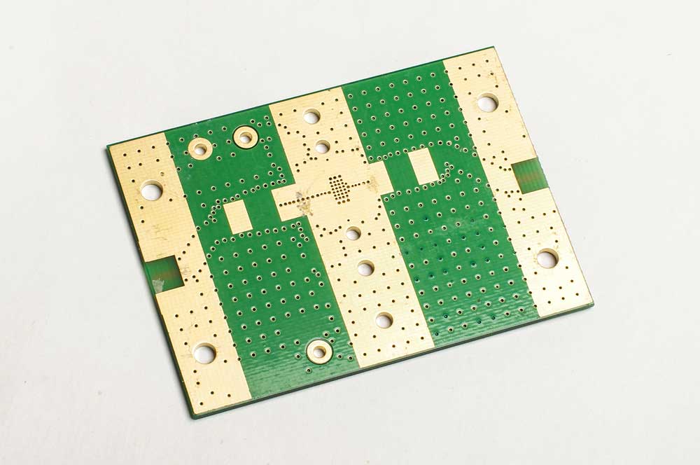
Double-sided through-hole PCB boards
Name: Double-sided through-hole PCB boards
Sheet: FR-4
Plate thICkness: 1.0mm
Layers: 2L
Size: 86.9*73.58mm
Minimum aperture: 0.236mm
Line width/moment: 0.32*0.37mm
Copper foil thickness: 1/1OZ
Surface treatment: lead-free spray tin
Solder mask/character: green oil white character
What is 2 layer PCB/double-sided PCB?
2 Layer PCBs are the most common type of PCB. Plus, 2 layer PCBs are also known as double-sided PCBs because they have components on both sides of the board.
The 2-layer pcb fabrication is by bonding two layers of copper together with a dielectric material in between. And the dielectric material can be either an FR-42 or an FR-44.
Furthermore, the copper on each side can carry different electrical signals, which makes them ideal for applications where high speed and/or dense packaging is necessary. 2 Layer PCBs are also the most economical type of PCB to manufacture.
How does a double-layer PCB work?
A 2 layer PCB works by having electrical signals routed between the two layers of copper. Interestingly, these signals can be either digital or analog. Plus, the dielectric material in the middle of the board helps to keep these signals from interfering with each other.
2 Layer PCB Thickness
So how thick is a 2 layer PCB?
A 2 layer PCB can be anywhere from 0.010” to 0.060” thick. In addition, the thickness of the board will depend on the dielectric material that you use and the size of the components mounted on the board. Also, the thicker the board, the better it is at reducing crosstalk between the signal traces.
2 layer board stack-up
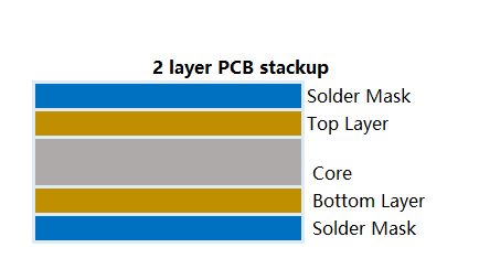
It's clear that layer 1, or the top layer is a signal layer on the 2 layers PCB stack up. Both the top layer and the bottom layer are copper layers.
inner layer
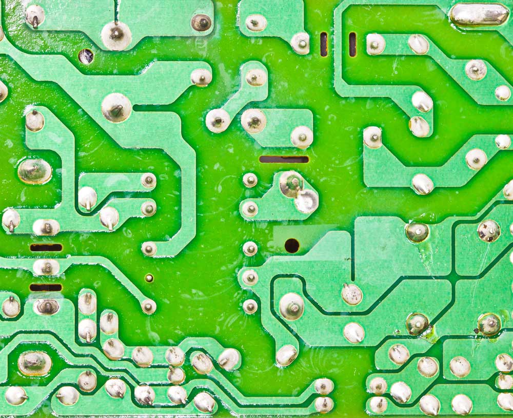
Electronic printed circuit board bottom layer
The 2-layer pcb has an inner layer which is also a copper layer. And this is where most of the vias get located. Plus, vias are the tiny little holes that connect the top and bottom layers together. More importantly, they allow for electrical signals to flow from one layer to another.
ground plane
The solid ground plane is to help reduce noise in electrical signals. Therefore, we can also use it to provide a place for the electrical signals to return. Besides that, it also helps to distribute heat better, and you can use it as a power or ground layer.
signal layers
The signal layers are the layers that carry the electrical signals. The 2 layer PCB has two signal layers, one for the top and one for the bottom. Usually, the top layer that we use for the signals that need to be routed on the outside of the board. While the bottom layer, you can use for the signals that need to be routed on the inside of the board.
power layer
The power layer we use to distribute power to the different parts of the board. Also, you can use it as a return path for the ground signals.
prepreg layer
The prepreg layer is a thin layer of dielectric material. And it can provide insulation between the copper layer. Besides, it can also provide support for the copper layers. The dielectric constant of the prepreg layer is 2. 2, which is lower than the FR-408 dielectric constant.
solder mask layer
The solder mask layer is a thin layer of material that covers the exposed copper. In addition, it can protect the copper from oxidation and corrosion.
silkscreen layer
The silkscreen layer is a thin layer of material that is used to print the legends on the board. Also, you can use it to print the board's name and part numbers.
How do You Make a 2-layer PCB /double-sided Circuit Board?
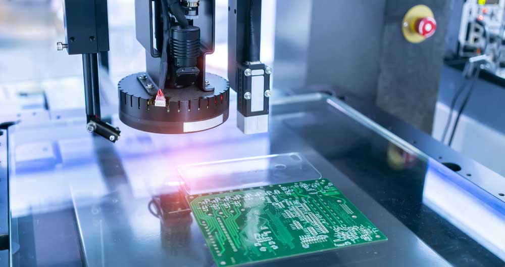
Vision measuring instrument inspecting PCB circuit board
To make a 2 layer PCB, you need to start with a substrate. And the most common substrate is FR-4. Once you have your substrate, you need to add the copper in layers.
The first layer you added is the signal layer. This is where it will carry the electrical signals.
The second layer you added is the ground layer. And this is where the electrical signals will return to it. Once you have your two copper layers, you need to add the prepreg layer.
The prepreg layer is an insulating material. As a result, It provides insulation between the layers.
After the prepreg layer, you need to add the solder mask. The solder mask is a thin layer of green or black plastic that helps to protect the copper from short circuits and corrosion.
Finally, you need to add the silkscreen. The silkscreen is a white or yellow printing on the PCB that shows the name of the components and their values.
2 Layer PCB Price
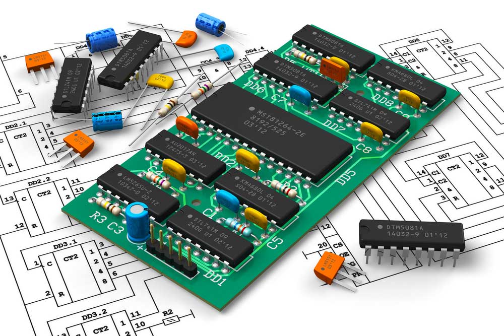
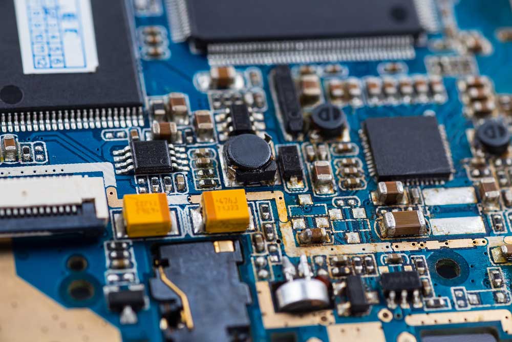
Digital circuit board with microchips
The price of a 2-layer PCB will vary depending on the size of the board, the complexity of the design, and the quantity that you order. Plus, 2-layer PCBs are typically more expensive than single-sided board because they require more materials and labor to manufacture.
The cost of a 2 layer PCB can range from $100 to $1000 per square foot. So, if you need a 2-layer PCB that is 2 feet by 2 feet, it would cost between $400 and $4000.
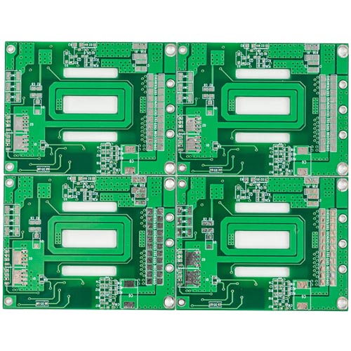
Name: Double-sided through-hole PCB boards
Sheet: FR-4
Plate thICkness: 1.0mm
Layers: 2L
Size: 86.9*73.58mm
Minimum aperture: 0.236mm
Line width/moment: 0.32*0.37mm
Copper foil thickness: 1/1OZ
Surface treatment: lead-free spray tin
Solder mask/character: green oil white character