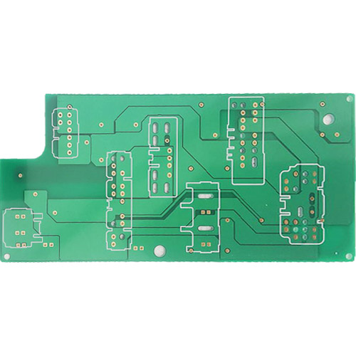
nickel-palladium-gold double-sided PCB
Name: nickel-palladium-gold double-sided PCB
Plate: KB6160A
Plate thickness: 1.6mm
Layers: Double-sided
Size: 49.6*32.8mm
Minimum aperture: 0.27mm
Line width/moment: 0.27*0.3mm
Copper Foil Thickness: 1 oz
Surface Treatment: Nickel Palladium Gold
Solder mask/character: green oil white character
Electroless nickel palladium gold is an important surface treatment process in the printed circuit board industry. It is widely used in the production process of hard circuit boards (PCB), flexible circuit boards (FPC), rigid scrambling boards and metal substrates. It is also an important development trend of surface treatment in the printed circuit board industry in the future.
1. Electroless nickel palladium gold
Electroless nickel palladium gold is a non-selective surface treatment technology that deposits a layer of nickel, palladium and gold on the surface of the copper layer of the printed circuit by chemical methods. The main process flow is degreasing - micro-etching - pre-dipping - activation - nickel plating - palladium plating - gold plating - drying. There will be multi-stage washing treatment between each link. The mechanism of electroless nickel-palladium-gold reaction mainly includes redox reaction and displacement reaction. Among them, the reduction reaction is easier to deal with thick palladium and thick gold products.
At present, the production specifications of chemical nickel, palladium and gold in general factories are: nickel 2-5um, palladium 0.05-0.15um, and gold 0.05-0.15um. Of course, due to differences in plant equipment and reaction mechanisms, the uniformity of chemical reactions and the ability to handle thick palladium and thick nickel are also different.
2. Electroless nickel palladium gold VS electroplating nickel gold
It is also an important surface treatment process in the field of printed circuit boards; the main application field is wire bonding technology, which can cope with high-end electronic circuit products to a certain extent.
3. Although chemical nickel-palladium-gold has a slow reaction speed, since it does not require the connection of lead wires and electroplating wires, the number of products produced simultaneously in the same volume of tank is much larger than that of electroplating nickel-gold, so the overall production capacity is very large. Advantage.
4. Development Trend
As mentioned earlier, the main advantage of electroless nickel palladium gold is to deal with the surface treatment of high-end products and fine circuits. However, the development of electronic technology and its attendant demands are also growing rapidly. At present, the common chemical nickel-palladium-gold process will gradually become incapable of coping with the production of high-precision circuits. Therefore, in order to cope with higher demand, the current main development direction is thin nickel palladium gold technology and chemical palladium gold technology.
Widely used in: communication, consumer electronics, industrial control, security, automobile, power supply, smart home, medical, military and other industries.
Name: nickel-palladium-gold double-sided PCB
Plate: KB6160A
Plate thickness: 1.6mm
Layers: Double-sided
Size: 49.6*32.8mm
Minimum aperture: 0.27mm
Line width/moment: 0.27*0.3mm
Copper Foil Thickness: 1 oz
Surface Treatment: Nickel Palladium Gold
Solder mask/character: green oil white character