
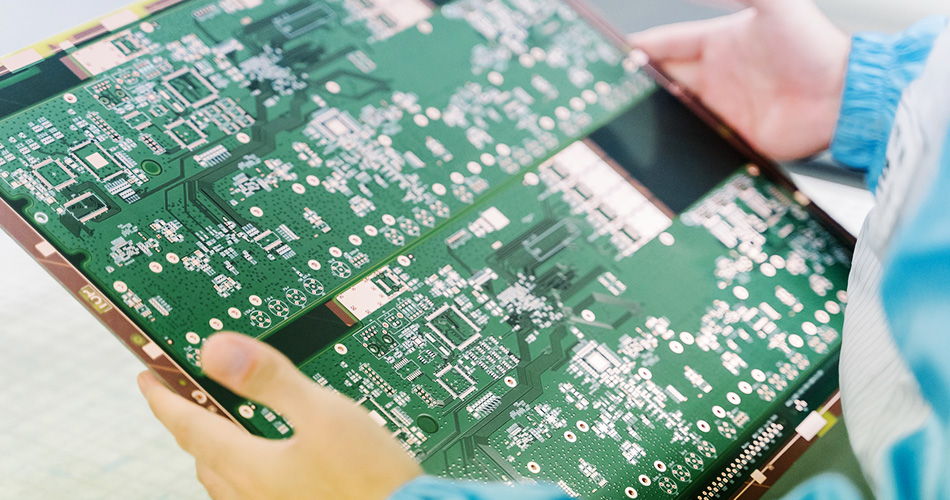
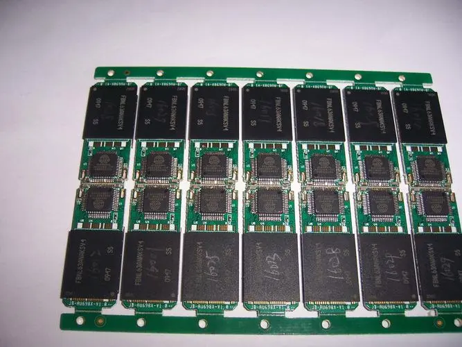
Professional PCB manufacturing and assembly
Building 6, Zone 3, Yuekang Road,Bao'an District, Shenzhen, China
+86-13410863085Mon.-Sat.08:00-20:00

The whole process of PCB copying
The technical realization process of PCB copying is simple, that is, first scan the circuit board to be copied, record the detailed position of the components, then disassemble the components to make a bill of materials (BOM) and arrange material procurement, then scan the blank board into a picture and restore it to a PCB drawing file after being processed by the board copying software, and then send the PCB file to the plate making factory to make the board. After the board is made, weld the purchased components to the made PCB board, Then it can be tested and debugged by the circuit board.
1、 Specific steps of PCB copying
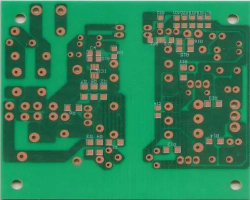
1. Get a PCB, and first record the models, parameters, and positions of all elements on the paper, especially the directions of diodes, transistors, and IC notches. It is better to take two photos of the position of the pneumatic parts with a digital camera. Now the pcb circuit board is becoming more and more advanced, and the diode triode on it is not noticeable.
2. Remove all the multilayer board copying parts and remove the tin in the PAD hole. Clean the PCB with alcohol, and then put it into the scanner. When the scanner scans, it needs to slightly increase the scanning pixels to get a clearer image. Then polish the top layer and bottom layer slightly with water gauze until the copper film is bright, put it into the scanner, start PHOTOSHOP, and sweep the two layers in color. Note that the PCB must be placed horizontally and vertically in the scanner, otherwise the scanned image cannot be used.
3. Adjust the contrast and lightness of the canvas to make the part with copper film contrast strongly with the part without copper film, and then turn the secondary image to black and white to check whether the lines are clear. If not, repeat this step. If it is clear, save the picture as black and white BMP files TOP.BMP and BOT BMP. If you find a problem with the graphics, you can also use PHOTOSHOP to repair and correct it.
4. Convert two BMP files into PROTEL files, and call in two layers in PROTEL. If the positions of PAD and VIA passing through two layers basically coincide, it indicates that the previous steps are well done. If there is any deviation, repeat the third step. Therefore, pcb board copying is a very patient work, because a small problem will affect the quality and the matching degree after board copying.
5. Convert BMP of TOP layer to TOP PCB, pay attention to convert to SILK layer, which is the yellow layer. Then you can trace lines on TOP layer, and place devices according to the drawing in step 2. Delete SILK layer after drawing. Repeat until all layers are drawn.
6. In PROTEL, call TOP.PCB and BOT.PCB, and it is OK to combine them into a picture.
7. Use the laser printer to print TOP LAYER and BOTTOM LAYER on the transparent film (1:1 ratio), put the film on that PCB, and compare whether there is any error. If it is correct, you will be finished.
A copy board like the original board was born, but it was only half finished. We also need to test whether the electronic technical performance of the copied board is the same as that of the original board. If it is the same, it is really finished.
Note: If it is a multilayer board, you should carefully polish it to the inner layer, and repeat the copying steps from step 3 to step 5 at the same time. Of course, the naming of the figure is different, and it should be determined according to the number of layers. Generally, the copying of double-sided boards is much simpler than that of multilayer boards, and the multi-layer boards are prone to misalignment, so the copying of multilayer boards should be particularly careful and careful (the internal through holes and non through holes are prone to problems).
2、 Method of copying double-sided board
1. Scan the upper and lower layers of the PCB and save two BMP images.
2. Open the board copying software Quickpcb2005, click "File" and "Open base map" to open a scan image. Use PAGEUP to enlarge the screen, see the pad, press PP to place a pad, see the line and press PT to route... Just like a child's drawing, draw it once in the software, and click "Save" to generate a B2P file.
3. Click "File" and "Open base map" again to open another layer of scanned color map;
4. Click "File" and "Open" again to open the previously saved B2P file. We can see that the board just copied is stacked on this picture - the same PCB board, the holes are in the same position, but the circuit connections are different. So we press "Options" - "Layer Settings", and turn off the display of lines and silk screen on the top layer here, leaving only multi-layer vias.
5. The vias on the top layer are in the same position as those on the bottom layer picture. Now we can trace the lines on the bottom layer as we did in childhood. Click "Save" again - the B2P file now has two layers of data: the top layer and the bottom layer.
6. Click "File" and "Export as PCB file" to get a PCB file with two layers of data, which can be changed or schematic diagram can be produced again or directly sent to PCB plate making factory for production.
3、 Multi layer board copying method
In fact, the four layer board copying is to copy two double-sided boards repeatedly, and the six layer board copying is to copy three double-sided boards repeatedly... The reason why the multi layer board is so daunting is that we cannot see its internal wiring. How can we see the inside of a precision multilayer board—— layered.
There are many layering methods, such as liquid medicine corrosion and tool stripping, but it is easy to divide the layers too much and lose data. Experience tells us that sandpaper grinding is the most accurate.
When we finish copying the top and bottom layers of PCB, we usually use sandpaper to polish the surface layer to show the inner layer; Sandpaper is a kind of ordinary sandpaper sold in hardware stores. Generally, the PCB is tiled, then the sandpaper is pressed and evenly rubbed on the PCB (if the board is very small, the sandpaper can also be tiled, and the PCB is pressed and rubbed on the sandpaper with a finger). The key point is to pave it so that it can be ground evenly.
The silk screen and green oil are usually wiped off, and the copper wire and copper skin should be wiped well. Generally speaking, the Bluetooth board can be wiped in a few minutes, and the memory module takes about ten minutes; Of course, with great strength, it will take less time; It will take a little more time.
Grinding plate is the most commonly used scheme for layering at present, and it is also the most economical. We can find an abandoned PCB to try. In fact, there is no technical difficulty in grinding the board, but it is a little boring. It takes some effort, and you don't have to worry about wearing the board to your fingers.
During PCB layout, after the system layout is completed, the PCB drawing shall be reviewed to see whether the system layout is reasonable and can achieve the optimal effect.
Generally, the following aspects can be considered:
1. Whether the system layout can ensure the reasonable or optimal wiring, whether it can ensure the reliable wiring, and whether it can ensure the reliability of circuit work. In the layout, it is necessary to have an overall understanding and planning of the signal direction and the power and ground network.
2. Whether the size of the printed board is consistent with the size of the processing drawing, whether it meets the requirements of PCB manufacturing process, and whether it has behavior marks. This requires special attention. The circuit layout and wiring of many PCB boards are designed beautifully and reasonably, but the precise positioning of the positioning connector is neglected, which makes the designed circuit unable to connect with other circuits.
3. Whether the components have conflicts in 2D and 3D space. Pay attention to the actual size of the device, especially the height of the device. The height of components without layout in welding shall not exceed 3mm generally.
4. Whether the layout of components is dense, orderly and orderly, and whether they are completely distributed. In the layout of components, it is not only necessary to consider the direction and type of signals, places needing attention or protection, but also the overall density of component layout to achieve uniform density.
5. Whether the components that need to be replaced frequently can be easily replaced, and whether the plug-in board can be easily inserted into the equipment. The replacement and connection of frequently replaced components shall be convenient and reliable.


Just upload Gerber files, BOM files and design files, and the KINGFORD team will provide a complete quotation within 24h.