
Professional PCB manufacturing and assembly
Building 6, Zone 3, Yuekang Road,Bao'an District, Shenzhen, China
+86-13410863085Mon.-Sat.08:00-20:00

For the success of a product, one must pay attention to the internal quality, and the other is to consider the overall aesthetics, both of which are perfect to consider the product to achieve success. On PCB board, the layout of pcb board design must be balanced and orderly, not top heavy or sinking. Let's take a look at some common questions that everyone has.
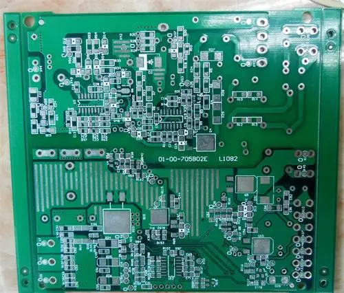
There are several problems in pcb board design. Professional pcb design company
First question:
Q: What methods can be used to eliminate electromagnetic interference in design?PCB
Answer: 1. Reduce loops: Each loop is equivalent to an antenna, so we need to minimize the number of cycles, the loop area, and the antenna effect of the loop. Ensure that the signal has only one loop path at any two points, avoid artificial loops and use the power plane as much as possible.
2. Filtering: filtering can be used on power lines and signal lines to reduce EMI. There are three methods: decoupling capacitors, EMI filters, and magnetic components.
3. Shielding. Because of the length of the question and many articles about the discussion,?? Didn't provide a more specific introduction.
4. Try to reduce the speed of high-frequency equipment.
5. Increase the dielectric constant of the PCB board to prevent the high-frequency part of the transmission line near the board from radiating outward; Increase the thickness of PCB board, minimize the thickness of microstrip lines, prevent electromagnetic lines from overflowing, and prevent radiation.
Second question:
Q: What aspects should be checked in the layout of the pcb board design?
Answer: In the design, the pcb layout is an important part. The quality of the layout results will directly affect the effect of the routing, so it can be considered that a reasonable layout is the first step to a successful PCB board design. There are two ways of layout, one is interactive layout, the other is automatic layout. Usually, the interactive layout based on automatic layout is used for adjustment. In the layout, the gate circuit can be reallocated according to the trace conditions, and two gate circuits can be exchanged to make it the best layout for wiring.
After the layout is completed, you can return and mark the design file and related information on the schematic diagram to make the related information on the PCB consistent with the schematic diagram, so as to create and modify the design in the future. Synchronize and perform the simulation at the same time. Update information to achieve board level verification of electrical performance and functions of circuits.


Just upload Gerber files, BOM files and design files, and the KINGFORD team will provide a complete quotation within 24h.