
Professional PCB manufacturing and assembly
Building 6, Zone 3, Yuekang Road,Bao'an District, Shenzhen, China
+86-13410863085Mon.-Sat.08:00-20:00

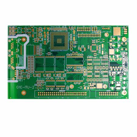
Why can't I make vias on pads? I just want to make them. What can I do? Many novices often encounter this problem when they first come into contact with PCB. Because the board space is too small and the devices are dense, the space is too small to lead the fan holes. They usually choose to punch the vias on the pad. Although it makes it easier for them to connect, they often do not know what problems will occur to the board? Can you fight like this?

In order to clearly explain this problem, the following two aspects will be elaborated:
1. Why can't vias be punched on pads?
In the early stage of PCB design, vias were not allowed on the BGA pad. The main reason was that the solder paste on the pad was not enough due to tin leakage, which would lead to false soldering and desoldering of devices during device welding. Therefore, generally, the holes on devices were made after the lead wire went out.
At this stage, due to the continuous narrowing of the BGA spacing, there will be no tin leakage through the resin plug hole. However, if the vias are punched on the bonding pad, there is a risk of false soldering or falling off, the cost will increase, and the aesthetics of the PCB will also be affected. Therefore, this is generally not recommended.
"Monument" phenomenon often occurs in the reflow soldering process of CHIP components (such as chip capacitors and chip resistors). The smaller the component volume, the easier it will occur, such as 0201, 0402 and other small chip components. In the reflow soldering process of surface mount process, the SMD components produce the phenomenon shown in the figure. Because a section of the components is cocked up, leading to desoldering, it is generally called the "monument" phenomenon.
The "monument" phenomenon is caused by the unbalanced surface tension of the two welding ends of the component when the solder paste on the pads at both ends of the component is refluxed and melted, and the end with larger tension pulls the component to rotate along its bottom. For some small package patch resistors and capacitors, it is also better not to punch vias on the pad. The vias are punched on the edge of the pad, which is prone to stand on a tablet due to inconsistent tension at both ends of the pad.
2. Under what circumstances can vias be punched on pads?
1) Buried blind hole
Generally speaking, when the BGA pitch spacing is less than or equal to 0.5mm, it is difficult for the BGA to fan out and drill holes. In this case, blind hole drilling can be used to solve the problem.
Blind vias: Blind vias are vias that connect PCB inner layer wiring with PCB surface layer wiring. This hole does not penetrate the whole board. For example, only from the surface layer to the middle layer.
Buried vias: Buried vias are the vias that only connect the routing between the inner layers, so they cannot be seen from the PCB surface.
As blind holes only open the surface layer to the inner layer, but not all PCBs, there will be no tin leakage. Buried holes are directly drilled from the inside, so there is no such concern. The only problem is that the cost will be considered, and the manufacturing cost of buried blind holes will be greatly increased.
2) Heat dissipation via
In PCB design, the design shown in the figure below is often seen. It is commonly found in the recommended design of chips. It is required to punch holes on the thermal pad. This is a heat dissipation via for IC heat dissipation. Since there is no pin to be welded in the middle of the chip body, there is no need to consider tin leakage, faulty soldering and other issues for the via on the IC heat dissipation pad.


Just upload Gerber files, BOM files and design files, and the KINGFORD team will provide a complete quotation within 24h.