
Professional PCB manufacturing and assembly
Building 6, Zone 3, Yuekang Road,Bao'an District, Shenzhen, China
+86-13410863085Mon.-Sat.08:00-20:00

PCB design is both science and art. There are many technical specifications related to wiring line width, wiring stack, schematic diagram, etc., but when you refer to the layout of components with artistic characteristics in PCB design, the problem becomes interesting.
In fact, there are few restrictions on the placement of components, and there is no "absolutely correct" specification requirement. This also makes the novice electronic engineer look like a full "second in the line" when handling the components on the circuit board, yearning for personal ambition and creativity. How to place the components depends entirely on you and the design idea.
However, this does not mean that you can do whatever you want. The design in the computer still needs to fall into the dust to form specific usable objects. Therefore, the following ten suggestions on the placement of PCB components can guide electronic beginners to complete the initial stage of electronic design smoothly.
Why is component placement so important?
It is true that 90% of PCB design is in device layout and 10% in wiring. Starting to put devices with great care can achieve twice the result with half the effort, and also can improve the electrical characteristics of PCB. If you just randomly place components on the circuit board, what will happen?
Time is wasted: It is very likely that you will find that there is no enough space for wiring in some places during the wiring process, or even the entire wiring needs to be replaced.
The circuit board does not work: you thought you would be all right if you placed the components and laid all the leads. Send the design documents to the circuit board manufacturer, and wait a few days to receive new circuit boards. When I was about to weld the circuit in high spirits, I was hit hard by the reality and found that some devices could not be welded at all (either the packaging was wrong or they were in conflict with each other).
Aesthetics is broken: we must admit that even though we are humble electronic engineers, we still agree with symmetry and meticulousness in the pursuit of aesthetics. The circuit board that was placed by people who lacked love and didn't mind at the beginning will be more congested in the later welding and debugging process. Only Ge Youtan can see it.
If you meet a professional, you will argue with you about the placement of components and the rules. For the same circuit diagram, 100 electronic engineers will have 1000 wiring schemes. This is why circuit board design is more regarded as the process of artistic creation.
If you always want to find out what is right and what is wrong, here is a tip to help you determine whether your circuit board components are properly placed. After the placement of components, use the automatic wiring in the circuit board design software (such as the one provided in Autodesk EAGLE) for wiring. If the final circuit failure rate is less than 85%, it means that you need to spend more time to optimize the placement of components.
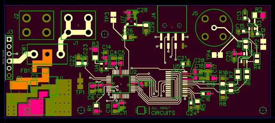
Tip 1: Understand the physical limitations of the circuit board
Before placing components, it is necessary to know exactly the mounting hole of the circuit board, the position of the edge connector and the mechanical size limit of the circuit board.
Because these factors affect the size and shape of your circuit board. I have seen that a circuit board designed by someone cannot be installed in the fixed area of the circuit board, so I had to redesign it.
In order to avoid foolishness, you can deliberately set a clear area for those mechanical restrictions (mounting holes, external contour of the circuit), so that you can rest assured that you can create within the allowable range.
Tip 2: Clarify the circuit board manufacturing process
Similarly, before placing circuit components, you'd better find out several key information from the circuit manufacturer:
1. Circuit assembly process and test flow;
2. Whether it is necessary to reserve space for PCB V-notch;
3. Component welding process: wave soldering, zone soldering or manual soldering?
The manufacturing process of circuit board will affect the gap size between components. In addition, if your circuit board will be welded on the assembly line in the future, you need to leave extra space (more than 20mil) at the edge of the circuit board for fixing the circuit board on the conveyor belt. The additional fixed plate on the circuit board, which is broken off after the circuit board is welded.
Tip 3: Leave breathing space for integrated chips
Note that the "breathing" here is not air. As for what it is, you will know after reading the following.
When arranging any components, it is necessary to leave a distance of at least 350mil between them as far as possible. For chips with many pins, the space needs to be larger.
Now there are more and more chip pins, and they are more and more dense. If the integrated chips are too close to each other, it is very likely that their leads cannot be easily led out and wired. It is often more difficult to wire later. Sometimes it will consume 100 of your hair if you take the trouble to arrange a wire. Even it is difficult to call every day. (If I had known this, why should I have done it in the first place)
Tip 4: Same device direction
For the same devices, let them line up as much as possible to keep consistent formation.
This is mainly to facilitate the assembly, inspection and test of the circuit board in the later stage, especially for the surface packaged devices, during the wave soldering process, the circuit board passes through the melting solder wave peak at a uniform speed. Uniformly placed devices have a uniform heating process, which can ensure high solder joint consistency.
Tip 5: Reduce lead crossing
By adjusting the device position and direction, lead wire crossing is reduced.
Now many PCB design software will provide a function to display the connection relationship between pin pairs without routing. By changing the position and direction of devices and minimizing the cross of leads between devices, a lot of energy can be saved for the subsequent wiring.
Tip 6: Place circuit edge devices first
The devices that cannot be moved arbitrarily due to mechanical restrictions should be placed first, such as external connectors, switches, USB ports, etc. on the circuit board.
These devices are often located at the time of the overall mechanical design of the system and cannot be changed. After placing these devices, you will have a glorious starting point for the device arrangement behind you. Get rid of the edge devices of the circuit board, and the rest is the highlight time for you to exert your imagination and creativity.
Tip 7: Avoid conflicts between devices
It is absolutely forbidden to overlap and share the bonding pads of components or overlap the edges of components for wiring in small circuit boards. It is better to keep a distance of 40 mil (1 mm) between all devices.
The most important reason is to avoid short circuit fault between pads in the later circuit manufacturing process. Remember, tight placement also makes wiring more difficult.
Similarly, the vias should be placed in a manner that is not too dense. These small round holes may also expose copper skin in the future, causing short circuit of the circuit.
Tip 8: Put the devices on the same side as much as possible
If you design a two-layer circuit board, the most common suggestion is to place the components on the same side.
If the components are not placed on the same side of the circuit board, it will make the late circuit board production laborious. Here's why. Normally, the components on the circuit board are placed by the automatic component placement machine. The components are only on one side, and the PCB production process only needs one time. Otherwise, the device shall be placed twice. To waste production time is to waste money and life.
Tip 9: Keep the chip pin and device polarity consistent
Each integrated chip has a mark indicating the starting position of pin 1. The same orientation of pin 1 of the chip, or the same orientation of polar devices (motor capacitor, diode, triode, LED, etc.), will also facilitate the production of the circuit board.
If you have soldered or debugged the circuit board yourself, you will not doubt this. Think about it. When you solder the components on the circuit board, the polarity and direction are very messy. Do you have no idea about successfully soldering the circuit board?
Tip 10: Device location is similar to the schematic diagram
When placing components, place them in your mind according to the position relationship on your schematic diagram.
In fact, you have already optimized the position relationship between components (the shortest connection and the least cross) when designing the schematic diagram. Therefore, follow the component position on the schematic diagram until the placement of PCB components is naturally reasonable. Especially, when wiring manually in the later stage, the schematic diagram in your mind will also help you secretly choose a reasonable short circuit path for wiring.
Creation under constraint
The best PCB design originates from the extraordinary layout of devices, so don't fool around. You should always focus on the rational placement of components. This process is worth all your efforts. This may be the most worthwhile process in PCB design. It will be a happy time to taste the fruits of labor when you see the design PCB become a finished circuit board.


Just upload Gerber files, BOM files and design files, and the KINGFORD team will provide a complete quotation within 24h.