
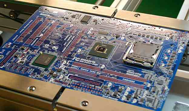
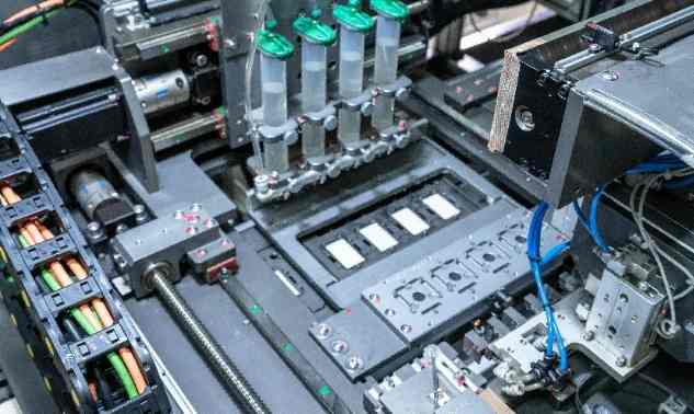
Professional PCB manufacturing and assembly
Building 6, Zone 3, Yuekang Road,Bao'an District, Shenzhen, China
+86-13410863085Mon.-Sat.08:00-20:00

As the diameter of the pilot hole becomes smaller and the thickness to diameter ratio becomes higher, it becomes more difficult to ensure that the metal in the hole is well covered. It is also challenging to ensure the uniformity of the metal in the hole and to protect the metal in the hole from etching during the mask and etching process after the graphic plating. In this paper, many causes of cavity in through hole copper layer are listed, and how to identify the root problem and discuss some suggestions on production process to avoid these problems.
Due to different reasons, the conductive layer cavity in the through hole shows different characteristics, but there is one thing in common, that is, the conductive layer in the hole is insufficient or no metal covering. Theoretically, the problem can be caused by either not enough metal being deposited or, after a sufficient amount has been deposited, part of the metal is lost for some reason. Inadequate metal deposition may be caused by improper plating parameters, such as the chemical composition of the tank, cathode movement, current, current density distribution, or plating time. This may also be because there are foreign bodies on the surface of the pore wall that prevent metal deposition, such as bubbles, dust, cotton fibers or organic membranes, sticky stains, etc. If the surface of the hole wall is not properly treated, it is not conducive to the deposition of the bath, it may also lead to bad metal deposition, such as: rough drilling, the formation of cracks, or a "pink circle".
"The removal of copper from the through-hole can be caused by chemical factors, such as etching, or mechanical causes, such as blow-holing, stress cracking, or deposition detachment.
In this paper, these defects and their causes are analyzed according to the steps along the through hole metallization process sequence where problems may occur and lead to holes in the hole. And draw lessons from the classical problem analysis to solve the useful factors, such as identifying the shape of the hole, location, and so on, and point out the method to correct the problem.

1. Factors that may lead to holes in the pre-metallization steps:
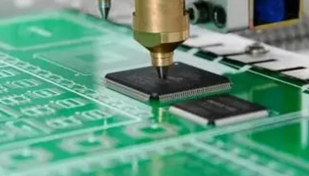
A. Drilling
A worn bit or other improper drilling parameters may tear the copper foil and dielectric layer, creating cracks. Glass fibers can also be torn rather than cut. Whether the copper will tear from the resin depends not only on the quality of the borehole, but also on the strength of the bond between the copper foil and the resin.
A typical example is that the bonding between the oxide layer and the semi-cured sheet is often weaker than that between the dielectric substrate and the copper foil, so most tearing occurs on the surface of the oxide layer of the multilayer. In metallography, tearing occurs on the smoother side of copper foil unless it is "revers treated foil." Poor bonding of the oxide surface to the semi-cured sheet can also lead to a worse "pink ring", where the oxide layer of copper dissolves in the acid. Rough borehole walls or rough, pink rings in the walls of holes can lead to holes at multilayer junctions called wedge woids or blow holes. "Wedge holes" are initially at the junction. Their name also suggests that they are shaped like "wedges" and retreat to form voids that can often be covered by electroplating. If the copper layer covers these ditches, there will often be moisture behind the copper layer. In later processes, such as hot air conditioning and high temperature treatment, moisture (moisture) evaporation and wedge holes usually occur together. It can be easily identified and distinguished from other types of voids by their location and shape.
Decontamination step is to remove the resin greasy stain on the inner copper by chemical method. The stain was originally caused by drilling. Cavitation is the further deepening of decontamination, which is to remove more resin, so that copper "protrude" from the resin, and form "three-point combination" or "three-side combination" with the copper plating layer, to improve the interconnection reliability. Permanganate is used to oxidize resins and "etch" them. The resin first needs to be swollen so that it can be treated with permanganate.
The neutralization step can remove the manganese residue. The glass fiber is etched using a different chemical method, usually hydrofluoric acid. Improper decontamination can result in two types of cavities: rough resin fouling on the pore wall may contain liquid, which can lead to "blow holes". Residual muck on the inner copper layer can prevent good bonding of the copper/copper coating, resulting in "hole wall pullaway", such as separation of the copper coating from the hole wall during high temperature treatment, or related testing.
Resin separation may lead to pore wall pulling and cracking and cavity in copper plating layer. If the potassium manganate residue is not completely removed in the neutralization step (to be precise 5, when it is a reduction reaction), it may also lead to cavitation. Reduction reactions often use reducing agents, such as hydrazine or hydroxylamine.


Just upload Gerber files, BOM files and design files, and the KINGFORD team will provide a complete quotation within 24h.