
Professional PCB manufacturing and assembly
Building 6, Zone 3, Yuekang Road,Bao'an District, Shenzhen, China
+86-13410863085Mon.-Sat.08:00-20:00

It is estimated that 25% to 30% of PCBS currently use organic coating processes, and this proportion is increasing (it is likely that organic coating is now in first place, ahead of hot air smoothing). The organic coating process can be used on low - and high-technology PCBS, such as PCB for single-sided TV sets and high-density chip packaging boards. For BGA, the application of organic coating is also more. If there are no surface connection functional requirements or storage life limits, organic coating is the most ideal surface treatment process.
1. Electroless nickel plating/gold leaching
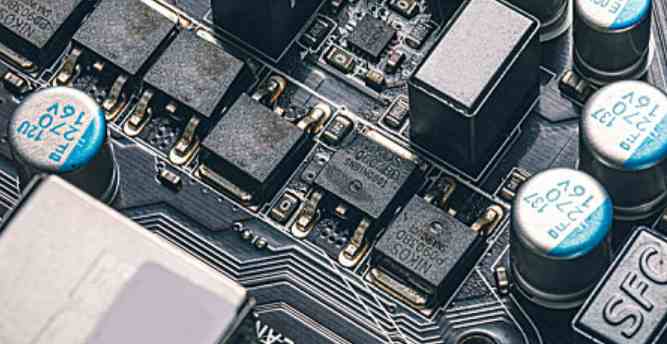
Unlike organic coating, the electroless nickel plating/gold plating process is mainly used on boards with surface connection functional requirements and long storage life, such as the key area of mobile phones, the edge connection area of router housing and the electrical contact area of the elastic connection of chip processors. Electroless nickel plating/gold dipping was widely used in the 1990s due to the flatness of hot air leveling and the removal of organic coated flux. Later, the use of electroless nickel plating/gold leaching process declined due to the advent of the black disc, brittle nickel-phosphorus alloy, but today almost every high-tech PCB plant has electroless nickel plating/gold leaching line.
Considering that the solder joint becomes brittle when the copper tin intermetallic compound is removed, the relatively brittle nickel tin intermetallic compound will present many problems. Therefore, portable electronic products (such as mobile phones) almost all use organic coated, silver or tin impregnated copper-tin intermetallic solder joints, while electroless nickel/gold plating is used to form key areas, contact areas and EMI shielding areas. It is estimated that 10% to 20% of PCBS currently use the electroless nickel/gold plating process.
2. Dip in silver
Silver immersion is cheaper than electroless nickel/gold plating, and is a good choice if the PCB has connection functional requirements and needs to reduce costs; Plus silver immersion good flatness and contact, it should be more choose silver immersion process. In communication products, automobiles, computer peripherals in a lot of applications, in high speed signal design also has applications. Silver immersion can also be used in high frequency signals because it has excellent electrical properties unmatched by other surface treatments. EMS recommends the silver immersion process because it is easy to assemble and has good inspectability. But it grows slowly (but does not decline) because of defects such as tarnish and holes in solder joints. It is estimated that 10% to 15% of PCBS currently use the silver leaching process.

Step 3 Dip tin
Tin was introduced into the surface treatment process in the last ten years. The appearance of the process is the result of the requirement of production automation. Tin immersion does not bring any element into the weld, especially suitable for communication backboard. Tin will lose its solderability outside the board's storage life, so better storage conditions are needed for leaching tin. In addition, tin leaching process is restricted because of carcinogenic substances. It is estimated that about 5-10% of PCBS currently use the tin leaching process.
V. Concluding remarks
It is impossible to predict exactly where PCB surface treatment technology will go in the future. With more and more high customer requirements, environmental requirements are more and more strict, surface treatment process is more and more, in the end the choice of the kind of development prospects, more universal surface treatment process, it seems a little dazzling, confusing. Anyway, to meet customer requirements and protect the environment must be done first!
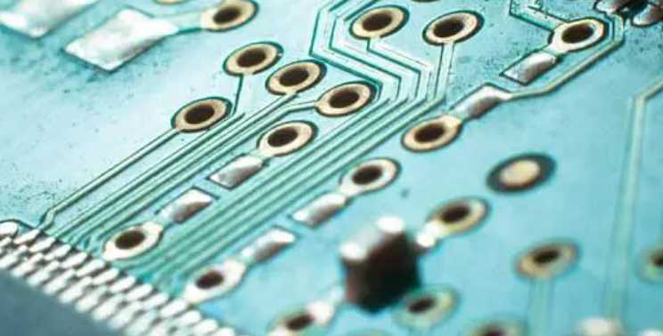
Why should PCB plug the hole?
In order to meet customer requirements, the Via hole must be plugged. After a lot of practice, the traditional aluminum sheet plugging process is changed, and the plate surface welding and plugging are completed with white mesh. Stable production and reliable quality.
The Via hole plays the role of connecting the lines to each other. The development of the electronics industry also promotes the development of PCB, which also puts forward higher requirements for the production process and surface mounting technology of printed board. Via hole plugging technology comes into being and should meet the following requirements:
(1) There is copper in the through hole, and welding resistance can be plugged or not plugged;
(two) there must be tin lead in the through hole, there is a certain thickness requirement (4 microns), no solder resistance ink into the hole, resulting in tin beads in the hole;
(three) the pass-through hole must have solder resistance ink plug hole, light proof, no tin ring, tin beads and flat requirements.
Why should PCB plug the hole?
With the development of electronic products to the direction of "light, thin, short, small", PCB also to high density, high difficulty development, so there are a large number of SMT, BGA PCB, and customers require plug holes when pasting components, mainly has five functions:
(a) To prevent PCB over wave soldering tin through the through hole through the component surface resulting in short circuit; In particular, when we put the hole on the BGA pad, we must first do the plug hole, and then gold-plated treatment, to facilitate the welding of BGA.
Why should PCB plug the hole?
(2) To avoid flux residue in the pass-through hole;
(3) After the completion of surface mounting and component assembly in the electronics factory, the PCB should be vacuated on the testing machine to form negative pressure:
(four) prevent the surface solder paste into the hole caused by virtual welding, affecting the installation;
(5) To prevent over wave soldering tin bead pop out, resulting in short circuit.
Four layer board design
Mar 30,2023


Just upload Gerber files, BOM files and design files, and the KINGFORD team will provide a complete quotation within 24h.