
Professional PCB manufacturing and assembly
Building 6, Zone 3, Yuekang Road,Bao'an District, Shenzhen, China
+86-13410863085Mon.-Sat.08:00-20:00

At present, the environmental problems involved in PCB productionare particularly prominent. Lead and bromine are the hottest topics at the moment; Lead-free and halogen-free will affect the development of PCB in many ways. Although at present, the changes in PCB surface treatment process are not very big and seem to be a relatively distant thing, it should be noted that long term slow changes will lead to great changes. In the case of environmental protection increasingly loud voice, PCB surface treatment technology will definitely change in the future.
I. Introduction
With the continuous improvement of human requirements for living environment, the environmental problems involved in PCB production are particularly prominent. Lead and bromine are the hottest topics at the moment; Lead-free and halogen-free will affect the development of PCB in many ways. Although at present, the changes in PCB surface treatment process are not very big and seem to be a relatively distant thing, it should be noted that long term slow changes will lead to great changes. In the case of environmental protection increasingly loud voice, PCB surface treatment technology will definitely change in the future.
Ii. The purpose of surface treatment
The most basic purpose of surface treatment is to ensure good solderability or electrical properties. Since natural copper tends to exist in the form of oxides in the air, it is unlikely to remain as raw copper for a long time, so other treatments are required for copper. Although strong flux can be used to remove most copper oxides in subsequent assembly, strong flux itself is not easily removed, so it is generally not used in the industry.
Three. Five common surface treatment processes
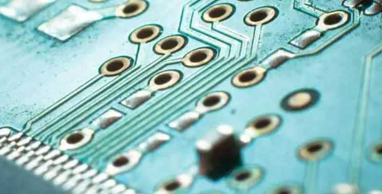
There are many PCB surface treatment processes. The common ones are hot air finishing, organic coating, electroless nickel plating/gold dipping, silver dipping and tin dipping, which are described below.

1. Hot air leveling
Hot air leveling, also known as hot air solder leveling, is a process of coating the PCB surface with molten tin lead solder and heating compressed air leveling (blowing), so that it forms a coating layer that is resistant to copper oxidation and can provide good solderability. Hot air conditioning solder and copper at the joint of the formation of copper tin gold compounds. The solder protecting the copper surface is approximately 1 to 2mil thick.
PCB for hot air polishing usually to soak in the molten solder; The air knife blows out the liquid solder before it sets; The air knife minimizes the meniscus of solder on the copper surface and prevents solder bridging. Hot air is divided into vertical type and horizontal type, horizontal type is generally considered to be better, mainly horizontal hot air leveling coating is more uniform, can realize automatic production. The general flow of hot air leveling process is: micro-etching → preheating → coating flux → tin-spraying → cleaning.
2. Organic coating
Organic coating process is different from other surface treatment process, it acts as barrier layer between copper and air; Organic coating is simple and inexpensive, which makes it widely used in the industry. The early organic coated molecules were imidazole and benzotriazole, which act as rust inhibitors. The latest molecules are mainly benzoidazole, which chemically bonds nitrogen functional groups to copper on PCBS. In the subsequent welding process, if only one layer of organic coating on the copper surface is not enough, there must be many layers. This is why liquid copper is often added to chemical tanks. After coating the first layer, the coating adsorbs copper; A second layer of organic coated molecules is then bonded to the copper until twenty or even hundreds of organic coated molecules have converged on the copper surface, thus guaranteeing repeated reflow soldering. The results show that the latest organic coating technology can maintain good performance in multiple lead-free welding processes.
The general flow of organic coating process is: degreasing → micro-etching → pickling → pure water cleaning → organic coating → cleaning, and the process control is easier than other surface treatment processes.
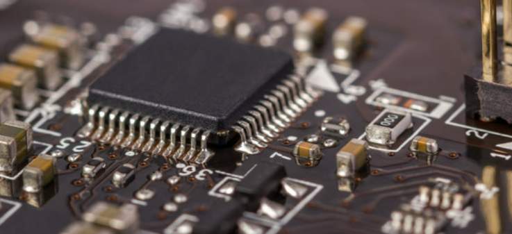
3. Electroless nickel plating/gold leaching
Electroless nickel plating/gold dipping process is not as simple as organic coating. Electroless nickel plating/gold dipping process is like wearing thick armor to PCB; In addition, unlike organic coating as an anti-rust barrier, electroless nickel plating/gold leaching process can be useful in the long-term use of PCB and achieve good electrical properties. Therefore, electroless nickel plating/gold leaching is to coat the copper surface with a thick layer of good electrical nickel gold alloy, which can protect the PCB for a long time; In addition, it has environmental tolerance that other surface treatment processes do not have. Nickel plating is due to the diffusion of gold and copper, and the nickel layer can prevent the diffusion of gold and copper; Without the nickel layer, the gold would diffuse into the copper within hours. Another benefit of electroless nickel plating/gold leaching is the strength of nickel, with a thickness of only 5 microns limiting Z-direction expansion at high temperatures. Electroless nickel/gold plating also prevents copper from dissolving, which would benefit lead-free assembly.
The general flow of electroless nickel plating/gold leaching process is: acid cleaning → micro-etching → preleaching → activation → electroless nickel plating → gold leaching. There are mainly 6 chemical tanks, involving nearly 100 chemicals, so the process control is difficult.
Why should PCB plug the hole?
Mar 30,2023


Just upload Gerber files, BOM files and design files, and the KINGFORD team will provide a complete quotation within 24h.