
Professional PCB manufacturing and assembly
Building 6, Zone 3, Yuekang Road,Bao'an District, Shenzhen, China
+86-13410863085Mon.-Sat.08:00-20:00


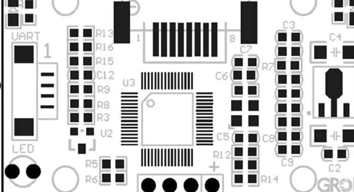
PCB surfaceneeds to be welded components, requires a part of the copper layer exposed for welding. These exposed layers of copper are called pads, which are usually rectangular or round and have a small area.
If the copper on the pad is oxidized, it is not only difficult to weld, but also increases the resistivity, which seriously affects the performance of the final product. So engineers came up with all sorts of ways to protect the pad. Such as plating the inert metal gold, or coating the surface with a layer of silver through a chemical process, or coating the copper layer with a special chemical film to prevent contact between the pad and the air.
Exposed pad on PCB, copper layer directly exposed. This part needs to be protected to prevent it from being oxidized.
From this point of view, whether gold or silver, the purpose of the process itself is to prevent oxidation, protect the pad, so that it in the following welding process to ensure yield.
However, the use of different metals will require the storage time and storage conditions of PCB used in the production factory. Therefore, PCB manufacturers generally use vacuum plastic sealing machines to pack PCBS before PCB production is completed and delivered to customers to ensure that PCB does not occur oxidation damage to the maximum extent.
And before the components on the machine welding, the board manufacturers also need to detect the oxidation degree of PCB, eliminate oxidized PCB, to ensure the yield. The final consumer gets the board card, has been through a variety of tests, even if the oxidation after a long time of use will almost only occur in the insertion and removal of the connection, and on the welding plate and have been welded components, there is no impact.
Since silver and gold have lower resistance, will the use of special metals such as silver and gold reduce the calorific value of the PCB?
We know that what affects the amount of heat is resistance; Resistance is also related to the material of the conductor itself, the cross-sectional area and length of the conductor. The thickness of metal material on the surface of the pad is even far less than 0.01mm. If the pad is treated with OST (organic protective film), there will be no excess thickness at all. The resistance of such a small thickness is almost zero, which is incalculable, and of course does not affect the calorific value.

Can PCB withstand 100 A current?
The usual PCB design current does not exceed 10A, even 5A. Especially in household and consumer electronics, usually the continuous working current on the PCB will not exceed 2A. However, to design the power wiring for the company's products recently, the continuous current can reach about 80A. Considering the instantaneous current and leave a margin for the whole system, the continuous current of the power wiring should be able to withstand more than 100A.
So the question is, what kind of PCB can withstand the current of 100 A?
Method 1: Routing cables on the PCB
To understand the PCB overcurrent capability, we start from the PCB structure.
Take a double-layer PCB, for example, which is usually a three-layer structure: copper, plate, copper.
Copper is PCB current, signal to pass through the path.
According to middle school physics knowledge can know an object's resistance and material, cross-sectional area, length.
Because our current is going through the copper, the resistivity is fixed. The cross-sectional area can be seen as the thickness of the copper skin, which is the thickness of the copper in the PCB processing options.
Copper thickness is usually expressed in OZ. 1OZ translates to 35 um, 2OZ is 70um, and so on.
It is easy to conclude, then, that in order to pass high currents on the PCB, the wiring should be short and thick, and the thicker the copper of the PCB, the better.
Actually in engineering, there is no strict standard for the length of wiring. In engineering, copper thickness/temperature rise/wire diameter are usually used to measure the current carrying capacity of PCB board.
The following two tables can be referenced:
It is known from the table that the circuit board is about 1OZ thick of copper, and the 100mil (2.5mm) width of the wire can pass 4.5A current at the temperature rise of 10℃.
In addition, with the increase of width, PCB current-carrying capacity does not increase strictly in line with the linear increase, but the increase range gradually decreases, which is also consistent with the actual project situation.
If the temperature rise is increased, the current carrying capacity of the wire can also be improved.
Through these two tables, the PCB wiring experience can be obtained: increasing copper thickness, widening wire diameter and improving PCB heat dissipation can enhance the current carrying capacity of PCB.
So if you want to run 100A current, you can choose 4OZ copper thickness, set the wire width to 15mm, double sided wire, and add heat dissipation device, reduce the temperature rise of PCB, improve the stability.
Method 2: Terminals
In addition to routing cables on the PCB, you can also route cables by using terminals.
Fix several 100A compliant terminals such as sheet nut, PCB terminal and copper post on the PCB or product housing.
Then the wire that can withstand 100A is connected to the terminal post with wiring terminals such as copper nose.
So that the large current can travel through the wire.
Method three: Custom copper bar
Even, it can be customized.
It is a common practice in industry to use copper bars to carry high current. For example, transformers, server cabinets and other applications all use copper bars to carry high current.


Just upload Gerber files, BOM files and design files, and the KINGFORD team will provide a complete quotation within 24h.