
Professional PCB manufacturing and assembly
Building 6, Zone 3, Yuekang Road,Bao'an District, Shenzhen, China
+86-13410863085Mon.-Sat.08:00-20:00

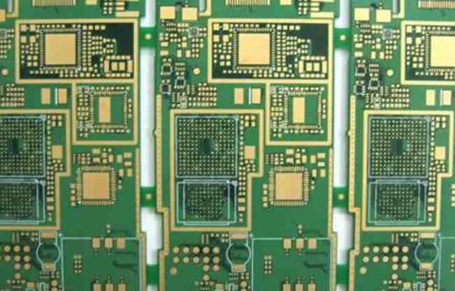
Since printed circuit boards are not your average terminal product, the definition of the name is somewhat confusing. For example, the motherboard of a personal computer is called a motherboard, not a circuit board. Although there's a board on the motherboard, it's not the same, so you can't say the same thing when you evaluate the industry. For example, the news media refer to integrated circuit components as IC boards because they are mounted on a circuit board, but in essence it is not equivalent to a printed circuit board. When we say a printed circuit board, we usually mean a bare board - a board with no upper components. In PCB board design and circuit board production, engineers not only need to prevent PCB board accidental encounters during the manufacturing process, but also need to avoid design errors.
1, circuit board short circuit: for this kind of problem, directly lead to the circuit board work one of the common faults, the biggest reason is PCB short circuit is the incorrect design of the pad. At this point, the circular pad can become oval. Shape to increase the distance between points to prevent short circuit. PCB proofing component direction design is not appropriate, will also lead to short circuit board and can not work. If the SOIC foot is parallel to the tin wave, it is easy to cause a short circuit accident. In this case, the orientation of the component can be modified to be perpendicular to the tin wave. PCBS can also be short-circuited, that is, automatically plug-in bending. Because the length of the wire specified by the IPC is less than 2mm, when the bending Angle is too large, the part may fall, so it is easy to cause short circuit, and the welding point needs to be more than 2mm off line.

2, PCB solder joints become golden: Generally speaking, PCB board solder is silver gray, but occasionally there will be gold solder joints. The main reason for this problem is that the temperature is too high, and it is only necessary to lower the temperature of the tin furnace.
3, black and granular contacts on the circuit board: Dark or small granular contacts on the PCB, mainly due to solder contamination and too much oxide in tin, forming too weak solder structure. Care must be taken not to confuse the dark color and low tin content caused by the use of solder. Another cause of the problem is the change in the composition of the solder itself used in the manufacturing process, which contains too much impurity and requires the addition of pure tin or replacement of solder. Tinted glass acts as a physical change in the fiber layers, such as separation between layers. However, this situation is not a bad solder joint. The reason is that the substrate heating is too high, need to reduce the preheating and welding temperature or improve the substrate travel speed.
4. Loose or misaligned PCB components: During reflow soldering, small components may float on molten solder and eventually fall out of the target solder joint. Possible causes of shift or tilt include vibration or rebound of components on soldered PCBS due to inadequate board support, reflow furnace setup, solder paste problems, human error, etc.
5, open circuit board: when the trace is broken or solder is only on the pad and not on the component lead, open circuit will occur. In this case, there is no glue or connection between the component and the PCB. Like short circuits, these can also occur during production or during welding and other operations. Shaking or stretching the board, dropping the board, or other mechanical deformation can damage the board or solder joints. In addition, chemicals or moisture can cause solder or metal parts to wear out, causing component wires to break.
6, welding problems: The following are some of the problems caused by poor welding: solder joint interference: solder before solidification due to external interference and move. This is similar to a cold weld spot, but can be corrected by reheating for different reasons, and the welded joint is cooled without external interference. Cold welding: This happens when the solder does not melt properly, resulting in rough surfaces and unreliable connections. Cold solder spots can also occur, as excess solder prevents full melting. The solution is to reheat the joint and remove excess solder. Welded bridge: This happens when solder crosses and physically joins the two leads together. These can create accidental connections and short circuits, which can cause the component to burn out or burn out the wires when the current is too high. Pad, needle or lead not wet enough. Too much or too little solder. A pad raised by overheat or rough welding.
7, PCB board is also affected by the environment: due to the structure of PCB itself when it is in an adverse environment, it is easy to cause damage to the circuit board. Extreme temperature or temperature changes, other conditions such as high humidity and high strength vibration are factors that lead to circuit board performance degradation or even obsolescence. For example, changes in ambient temperature can cause circuit boards to deform. This can break the solder joints, bend the shape of the board, or it can cause the copper wires on the board to break. On the other hand, moisture in the air can cause oxidation, corrosion and rust on metal surfaces such as exposed copper wires, solder joints, pads and component leads. Buildup of dirt, chips, or debris on the surfaces of components and boards can also reduce air flow and component cooling, which can cause the PCB to overheat and degrade performance. Vibration, drop, impact, or bending of the PCB can cause the PCB to deform and cause cracks to appear, while high current or overvoltage can cause damage to the PCB or cause rapid aging of components and paths.
8. Human error: Most defects in PCB manufacturing are caused by human error. In most cases, faulty production processes, incorrect component placement and unprofessional manufacturing specifications result in up to 64% avoidable. Product defect occurs.
Five PCB integrated circuit assembly methods
Feb 12,2023


Just upload Gerber files, BOM files and design files, and the KINGFORD team will provide a complete quotation within 24h.