
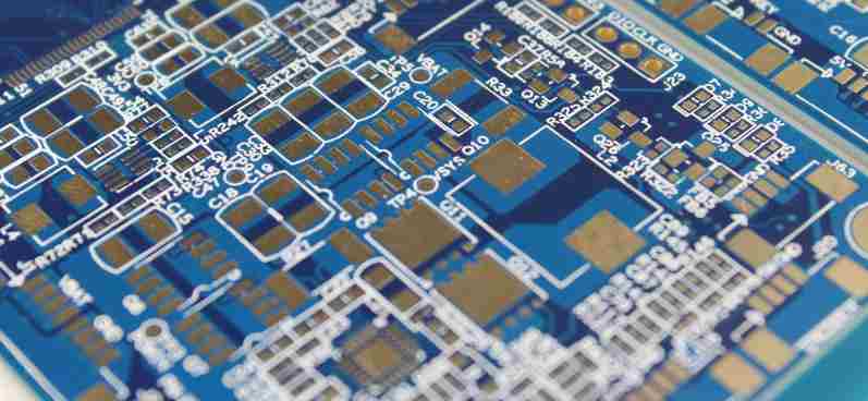
Professional PCB manufacturing and assembly
Building 6, Zone 3, Yuekang Road,Bao'an District, Shenzhen, China
+86-13410863085Mon.-Sat.08:00-20:00


Antenna use long strip PCB circuit board
Modern wireless applications require sturdy antennas, which often means a long printed circuit board to integrate and support these applications. Antenna designs can make or break your application, but relying on long PCBS can help you get the job done right.

The antenna can be mounted directly on the long printed circuit board, and the copper optimization design can improve its performance.
Antennas are often very difficult areas to design in, and working with experts can help you optimize the impact your circuit board has.
Antenna application
Almost every modern device uses wireless antennas, and these devices reach our homes. Everything from cell phones and coffee makers to new washing machines and television sets have an antenna that may be placed directly on the circuit board.
Printed circuit board antenna applications vary significantly according to signal strength and requirements, so you will see a variety of antenna designs in today's PCBS.
This loop is the most basic iteration of a long PCB antenna, where the manufacturer creates a closed copper wire loop connected to the antenna terminal. Loops don't have to be circular, but they do need to be as circular as possible, because larger means more efficient and better operation. You'll find loops in places that don't have efficient signal requirements, like your garage door remote control.
Patch antenna is a relatively efficient option for coaxial cable or micros trip production. Copper zone designs are common in WLAN networks due to strong support and narrow bandwidth. The thicker the dielectric material, the better the bandwidth.
Zigzag lines allow conductors to move from side to side to increase strength while limiting antenna size. Its radiation resistance and efficiency are somewhat reduced due to its design, but if size is a top concern, it might work just fine.
A slot antenna is a slot cut in a metal sheet or directly on the copper plane of a PCB. This is a complex design that requires matching, as its impedance averages around a few hundred ohms. This is a design often used for phase arrays.
Prevent bow and twist on PCB board
If the surface mount and through-hole components x/y and z coordinates do not match the pcb, then bow and twist problems on the printed circuit board can cause the components and parts to shift during the PCB assembly process, then it will make the PCB assembly process very time consuming and difficult.
IPC-6012 defines a maximum bend and twist on the board of 0.75%, but some strict designs only allow bending and twisting no more than 0.5%. See below for IPC guidelines on how to measure bows and twists.
Prevent bows and twists on the circuit board:
1. PCB design: If needed, PCB designers should use copper wire to balance the design between layers to evenly distribute copper.
2. Lamination: The prepreg between PCB layers must be symmetrical unless specific impedance requirements exist.
3. Multilayer printed circuit boards should use the same material manufacturer's core and prepreg, as different manufacturers may cause problems during lamination.
6. Printed circuit boards are very thin to twist and distort easily, so they should be observed in every process.
7. Bake the printed circuit board, making sure it is free of moisture, and place it on a flat surface during the cooling process.
8. Circuit boards are blind and embedded through holes are more likely to bend and bend, so they must be carefully handled and controlled during manufacturing.
Bow and twist problems occur not only during PCB manufacturing, but also due to uneven distribution of copper in Gerber files.
If impedance or special requirements are not required, board designers should design multilayer PCBS using symmetrical stacking. The weight of the copper should be symmetrical as well as the thickness of the prepreg and core.
9. Large processing procedures: A. Take out the anode, take off the anode bag, clean the anode surface with a copper brush, wash dry, into the anode bag, into the acid tank reserve B. Soak the anode bag in 10% lye for 6-8 hours, rinse and dry, then soak in 5% dilute sulfuric acid, rinse and dry for use; C. Transfer the tank to the standby tank, slowly dissolve the activated carbon powder into the tank at the rate of 3-5 g/l. After the thorough dissolution, adsorption for 4-6 hours, use 10um PP filter element and filter powder to filter the tank into the clean working tank, put in the anode, hung on the electrolytic plate, electrolytic for 6-8 hours at 0.2-0.5ASD current density low current, D. After laboratory analysis, adjust the content of sulfuric acid and stannous sulfate in the tank to the normal operating range; Tinning additives were added according to the results of Hall groove test. E. Stop electrolysis when the color of the electrolytic plate surface is uniform; F. Test plating OK.
PCB nickel plating
Feb 11,2023


Just upload Gerber files, BOM files and design files, and the KINGFORD team will provide a complete quotation within 24h.