
Professional PCB manufacturing and assembly
Building 6, Zone 3, Yuekang Road,Bao'an District, Shenzhen, China
+86-13410863085Mon.-Sat.08:00-20:00

PCBA welding processing, usually PCB board has a lot of requirements, and must meet the requirements of the board to accept welding processing. So, why does the welding process need to have so many requirements on the circuit board?
It has been proved that in the process of PCBA welding, there will be a lot of special technology, and the application of special technology immediately brings the requirements for PCB board, if there is a problem on PCB board,
It will increase the difficulty of PCBA welding process, which may eventually lead to welding defects, unqualified boards and other situations. Therefore, in order to ensure the smooth completion of the special process and facilitate the PCBA welding processing,
PCB board must be in size, pad distance and other aspects of manufacturability requirements.
PCBA welding processing of PCB board requirements have the following points:
1. PCB size
The width of the PCB (including board edges) must be greater than 50mm and less than 460mm, and the length of the PCB (including board edges) must be greater than 50mm. If the size is too small, it needs to be assembled.
2, PCB board edge width
Edge width > 5mm, plate spacing < 8mm, distance between plate and edge > 5mm.
3. PCB bending degree
Upward curvature: < 1.2mm, downward bending: < 0.5mm, PCB deformation: maximum deformation height ÷ diagonal length < 0.25.
4, PCB board Mark point
Mark shape: Standard circle, square, triangle
Mark size: 0.8~1.5mm
Mark materials: Gold, tin, copper and platinum
Mark's surface requirements: smooth surface, no oxidation, no dirt
Requirements around Mark: Within 1mm of the mark, there should be no obstacles such as green oil, which is obviously different from the color of the mark
Mark position: More than 3mm away from the edge of the plate, and no marks such as holes and test points shall be found within 5mm
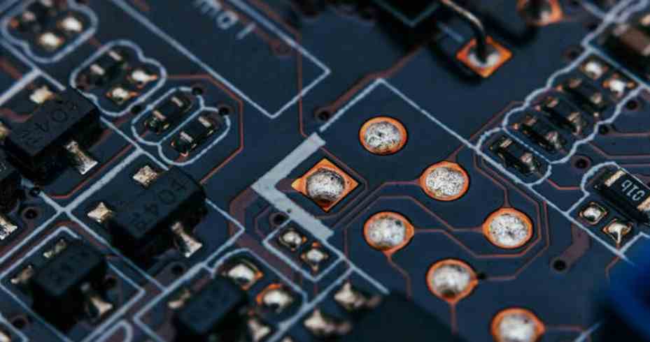
5. PCB welding pad
There is no through hole on the patch component pad. If there is a through-hole, the solder paste will flow into the hole, resulting in less tin in the device, or the tin flow to the other side, resulting in uneven surface, unable to print solder paste.
When designing and manufacturing PCB, it is necessary to know some knowledge of PCB welding process in order to make the product suitable for production. Understanding the requirements of the processing plant first can make the subsequent manufacturing process more smooth and avoid unnecessary trouble.
This is the PCBA welding processing of PCB board requirements, in the production of PCB board is not slack, the production of high-quality compliance of the PCB board in order to let the board better accept other special processes, and give PCB board life, and inject the soul of function.
Design principles of SMT-PCB
I. Layout of components on SMT-PCB
1. When the circuit board is placed on the conveyor belt of the reflow welding furnace, the long axis of the components should be perpendicular to the transmission direction of the equipment, which can prevent the phenomenon of components drifting on the board or "erecting tablets" in the welding process.
2. PCB components should be evenly distributed, especially the high-power components should be dispersed to avoid local overheating stress on PCB when the circuit is working, affecting the reliability of solder joints.
3. For double-sided mounted components, staggered installation positions should be placed on larger devices on both sides, otherwise the welding effect will be affected by the increase of local heat capacity in the welding process.
3. Devices with pins on four sides such as PLCC/QFP can not be placed on the wave crest welding surface.
4. The long axis of the SMT large device installed on the crest welding surface should be parallel to the direction of the peak flow of the solder, which can reduce the solder bridge between electrodes.
5. The large and small SMT components on the wave crest welding surface should not be arranged in a straight line. The positions should be staggered, so as to prevent virtual welding and missing welding caused by the "shadow" effect of the solder crest during welding.

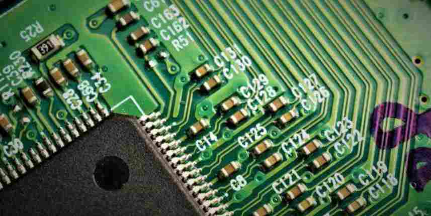
Two, SMT-PCB welding pad
1. SMT components on the wave soldering surface, the pad of the larger components (such as triode, socket, etc.) should be appropriately enlarged, such as the pad of SOT23 can be lengthened 0.8-1mm, so as to avoid the air welding caused by the "shadow effect" of the components.
2, the size of the pad should be determined according to the size of the components, the width of the pad is equal to or slightly greater than the width of the electrode of the components, the best welding effect.
3, between the two connected components, to avoid using a single large pad, because the solder on the big pad will connect the two components to the middle, the correct way is to separate the two components of the pad, in the middle of the two pad with a thinner wire connection, if the wire through the larger current can be connected in parallel with several wires, the wire covered with green oil.
4. There shall be no through hole on or near the pad of SMT components; otherwise, in the REFLOW process, the solder on the pad will flow away along the through hole after melting, resulting in virtual welding, less tin, and possibly flowing to the other side of the plate, causing short circuit.
PCB hole copper design principles for PCB design
Feb 10,2023


Just upload Gerber files, BOM files and design files, and the KINGFORD team will provide a complete quotation within 24h.