
Professional PCB manufacturing and assembly
Building 6, Zone 3, Yuekang Road,Bao'an District, Shenzhen, China
+86-13410863085Mon.-Sat.08:00-20:00

With the rapid development of electronic and communication products, signal transmission volume increases and transmission speed is accelerated, which makes the direction of high frequency, high power and miniaturization. High signal power, high current and high voltage put forward higher requirements for PCB surfacecopper degree and hole copper thickness.
What is pore copper?
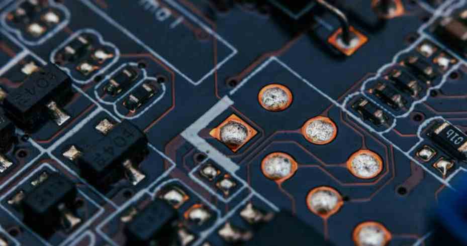
Speaking of this, I believe some people do not know what pore copper is. The so-called pore copper is the hole with metalization requirements. Through electroplating, a layer of copper is plated inside the hole, so that both sides of the hole can be conductive.
In the process of PCB board making, the thickness of the copper through the hole is not uniform, and the copper through the local hole of the PCB is too thin, which leads to the fracture of the copper through the hole during reflow welding due to the influence of heat shock, resulting in the failure of the open circuit.
Through-hole electroplating is a very important link in the process. In order to provide electrical connection for conductive metals of different levels, it is necessary to coat the wall of through-hole with metal copper with good conductivity.
With the increasingly fierce competition of terminal products, the reliability of PCB products is bound to put forward higher requirements, and the thickness of through-hole electroplating has become one of the items to measure the reliability of PCB. That is to say, an important reason affecting PCB hole copper thickness is PCB electroplating deep plating ability.
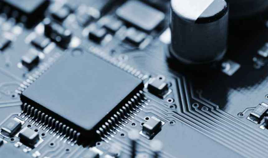
With the rapid development of electronic products in the direction of portable, miniaturized, networked and multi-media, higher requirements are put forward for the surface mounting technology of electronic components.
PCB hole copper design principles for PCB design
With the rapid development of electronic and communication products, signal transmission volume increases and transmission speed is accelerated, which makes the direction of high frequency, high power and miniaturization. High signal power, high current and high voltage put forward higher requirements for PCB surface copper degree and hole copper thickness.
What is pore copper?
Speaking of this, I believe some people do not know what pore copper is. The so-called pore copper is the hole with metalization requirements. Through electroplating, a layer of copper is plated inside the hole, so that both sides of the hole can be conductive.
In the process of PCB board making, the thickness of the copper through the hole is not uniform, and the copper through the local hole of the PCB is too thin, which leads to the fracture of the copper through the hole during reflow welding due to the influence of heat shock, resulting in the failure of the open circuit.
Through-hole electroplating is a very important link in the process. In order to provide electrical connection for conductive metals of different levels, it is necessary to coat the wall of through-hole with metal copper with good conductivity.
With the increasingly fierce competition of terminal products, the reliability of PCB products is bound to put forward higher requirements, and the thickness of through-hole electroplating has become one of the items to measure the reliability of PCB. That is to say, an important reason affecting PCB hole copper thickness is PCB electroplating deep plating ability.
With the rapid development of electronic products in the direction of portable, miniaturized, networked and multi-media, higher requirements are put forward for the surface mounting technology of electronic components.
PCB hole copper design principles for PCB design
With the rapid development of electronic and communication products, signal transmission volume increases and transmission speed is accelerated, which makes the direction of high frequency, high power and miniaturization. High signal power, high current and high voltage put forward higher requirements for PCB surface copper degree and hole copper thickness.

What is pore copper?
Speaking of this, I believe some people do not know what pore copper is. The so-called pore copper is the hole with metalization requirements. Through electroplating, a layer of copper is plated inside the hole, so that both sides of the hole can be conductive.
In the process of PCB board making, the thickness of the copper through the hole is not uniform, and the copper through the local hole of the PCB is too thin, which leads to the fracture of the copper through the hole during reflow welding due to the influence of heat shock, resulting in the failure of the open circuit.
Through-hole electroplating is a very important link in the process. In order to provide electrical connection for conductive metals of different levels, it is necessary to coat the wall of through-hole with metal copper with good conductivity.
With the increasingly fierce competition of terminal products, the reliability of PCB products is bound to put forward higher requirements, and the thickness of through-hole electroplating has become one of the items to measure the reliability of PCB. That is to say, an important reason affecting PCB hole copper thickness is PCB electroplating deep plating ability.
With the rapid development of electronic products in the direction of portable, miniaturized, networked and multi-media, higher requirements are put forward for the surface mounting technology of electronic components.


Just upload Gerber files, BOM files and design files, and the KINGFORD team will provide a complete quotation within 24h.