
Professional PCB manufacturing and assembly
Building 6, Zone 3, Yuekang Road,Bao'an District, Shenzhen, China
+86-13410863085Mon.-Sat.08:00-20:00

1, what is a halogen?
In the periodic table of chemical elements, the periodic series Ⅶ element refers to the halogen element, including fluorine (F), chlorine (Cl), bromine (Br), iodine (I), astatine (At).
2, what is halogen-free circuit board?
According to JCA-ES-01-2003 (JPCA for short) standard, chlorine (Cl), bromine (Br) element content is less than 0.09% Wt(weight ratio), defined as halogen-free copper clad plate.
3, the halogen-free circuit board and we usually do the board is different?
At present, the circuit board market uses the flame retardant substrate FR4, CIM-1, CIM-3, etc., the flame retardant is mostly brominated epoxy resin. Related institutions have done research on epoxy resin substrate: when the flame retardant substrate containing halogen is discarded and burned, it will release dioxins and other harmful substances. This substance has an unpleasant smell, high toxicity, and can cause cancer. Once inhaled, the human body can not be discharged, which has great harm to the human body.
Halogen-free board is to replace or replace these harmful elements to achieve environmental protection and non-toxic PCB. At present, most halogen-free materials are mainly phosphorus series and phosphorus nitrogen series. Interestingly, the polymer resin containing phosphorus nitrogen compounds will produce non-combustible gas when it is burned. This gas can isolate the surface and air of the resin combustion, so as to achieve the purpose of flame retardant.
4. What are the advantages of halogen-free PCB?
Halogen-free PCB in addition to environmental protection, but also has good heat dissipation reliability, more suitable for lead-free circuit required high temperature process; As halogen-free PCB uses P or N to replace halogen atoms, the polarity of the molecular bond segment of epoxy resin is reduced to a certain extent, thus improving the insulation resistance and resistance to penetration.
Every coin has two sides, and the advantages of halogen-free plates come at the cost of complexity not only in the manufacturing process but also in the design. Halogen-free PCB board and conventional PCB have differences, such as drilling. The P and N series functional groups used in halogen-free plates increase the molecular weight and enhance the rigidity of molecular bonds, resulting in increased rigidity of materials. At the same time, the TG points of halogen-free materials are generally high, so the drilling effect of ordinary FR-4 drilling parameters is not ideal. When drilling a halogen free plate, make some adjustments under normal drilling conditions.
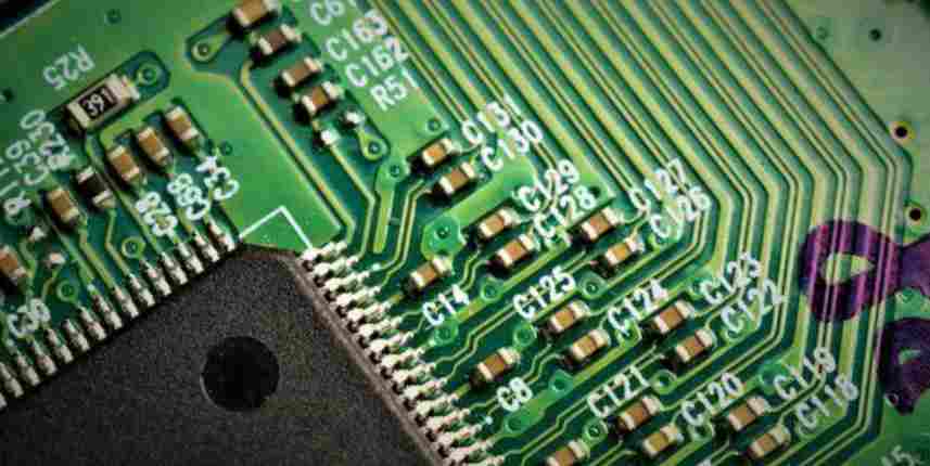
The circuit board is a number of layers, 1 layer called PCB single panel, 2 layers referred to as PCB double panel, 3-48 layers called PCB multilayer board, the higher the number of layers, the higher the unit price; PCB multilayer board and PCB dual panel in appearance,
It's pretty much the same. It's hard to tell. You may ask: Isn't a multilayer layer? How to see is also a board ah? So, how to distinguish PCB double panel and multilayer PCB board with the naked eye?
1. The more layers there are, the larger the shadow will be in the board;
2.PCB double panel has line and ink at both ends, careful observation can be identified;
3. There is no line visible in the PCB double panel board, and what is seen is pure board material and pure glass fiber;
4. If the board is die punch, you can use your hand to insert the edge of the board, so that the board is smooth and recognizable;
5. The multilayer PCB board board can see the faint shadow, a little dim or even dark, deep can basically see the inside of the line;
6. The multilayer PCB board material is usually the use of KB material, compared with the appearance of the double panel of the board is smooth, especially after the molding processing and cleaning can see the line inside;
7. The exact number of layers can only be identified by the manufacturer's IM inspection or the drawing record of the development engineer.
PCBA welding processing, usually PCB board has a lot of requirements, and must meet the requirements of the board to accept welding processing. So, why does the welding process need to have so many requirements on the circuit board?
It has been proved that in the process of PCBA welding, there will be a lot of special technology, and the application of special technology immediately brings the requirements for PCB board, if there is a problem on PCB board,
It will increase the difficulty of PCBA welding process, which may eventually lead to welding defects, unqualified boards and other situations. Therefore, in order to ensure the smooth completion of the special process and facilitate the PCBA welding processing,
PCB board must be in size, pad distance and other aspects of manufacturability requirements.

PCBA welding processing of PCB board requirements have the following points:
1. PCB size
The width of the PCB (including board edges) must be greater than 50mm and less than 460mm, and the length of the PCB (including board edges) must be greater than 50mm. If the size is too small, it needs to be assembled.
2, PCB board edge width
Edge width > 5mm, plate spacing < 8mm, distance between plate and edge > 5mm.
3. PCB bending degree
Upward curvature: < 1.2mm, downward bending: < 0.5mm, PCB deformation: maximum deformation height ÷ diagonal length < 0.25.
4, PCB board Mark point
Mark shape: Standard circle, square, triangle
Mark size: 0.8~1.5mm
Mark materials: Gold, tin, copper and platinum
Mark's surface requirements: smooth surface, no oxidation, no dirt
Requirements around Mark: Within 1mm of the mark, there should be no obstacles such as green oil, which is obviously different from the color of the mark
Mark position: More than 3mm away from the edge of the plate, and no marks such as holes and test points shall be found within 5mm
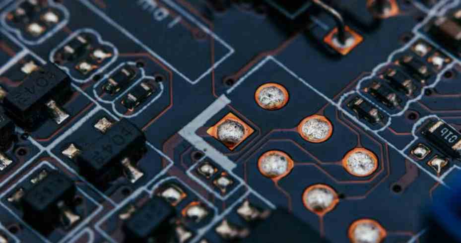
5. PCB welding pad
There is no through hole on the patch component pad. If there is a through-hole, the solder paste will flow into the hole, resulting in less tin in the device, or the tin flow to the other side, resulting in uneven surface, unable to print solder paste.
When designing and manufacturing PCB, it is necessary to know some knowledge of PCB welding process in order to make the product suitable for production. Understanding the requirements of the processing plant first can make the subsequent manufacturing process more smooth and avoid unnecessary trouble.
This is the PCBA welding processing of PCB board requirements, in the production of PCB board is not slack, the production of high-quality compliance of the PCB board in order to let the board better accept other special processes, and give PCB board life, and inject the soul of function.


Just upload Gerber files, BOM files and design files, and the KINGFORD team will provide a complete quotation within 24h.