
Professional PCB manufacturing and assembly
Building 6, Zone 3, Yuekang Road,Bao'an District, Shenzhen, China
+86-13410863085Mon.-Sat.08:00-20:00


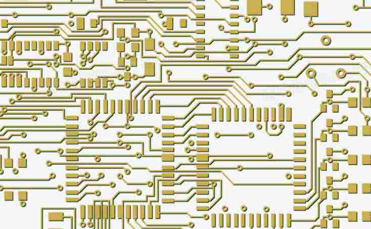
PCB circuit board in the process of proofing, sometimes found PCB electroplating layer black phenomenon. So, what is the cause of the black PCB electroplating layer?
1, plating nickel layer thickness control
PCB electroplated layer is generally a very thin layer, reflected in the electroplated surface of many problems caused by the poor performance of nickel plating. Generally, the thin nickel plating layer will cause the appearance of the product will be white and black phenomenon, so this is the first choice for engineering and technical personnel to check the project, generally need to electroplating to about 5μthickness of the nickel layer to solve the problem of white and black appearance.
2, electroplating nickel cylinder potion condition
If the nickel cylinder potion is not well maintained for a long time, no timely carbon treatment, then the plating out of the nickel layer will be easy to produce flake crystallization, resulting in increased hardness and brittleness of the coating, serious will produce black coating phenomenon. Therefore, engineering and technical personnel need to carefully check the production line potion condition, comparative analysis, and timely thorough carbon treatment, so as to restore the potion activity and electroplating solution cleanliness.
3. Gold cylinder control
As long as the good potion filtration and supplement are maintained, the contamination degree and stability of the gold cylinder will be better than that of the nickel cylinder, but engineering and technical personnel need to pay attention to check whether the following aspects are good:
(1) whether the VAT supplement is sufficient and excessive;
(2) Control of PH value of the potion;
(3) What is the situation of conductive salt?
If the result of the inspection by the engineering and technical personnel is no problem, then AA machine is used to analyze the content of impurities in the solution and the state of the deposit cylinder. Finally, don't forget to check whether the cylinder filter cotton core has not been changed for a long time.

PCB screen printing is an important link in PCB manufacturing process, then, what are the common failures of PCB screen printing?
A, the screen version of the fault
1. Plugging holes
The reasons for this kind of situation are: printing material dry too fast, in the screen version dry plugging hole, printing speed is too fast, scraper strength is too high. Solution, should use volatile organic solvent slow printing material, with soft cloth stained with organic solvent gently cleaning screen.
2, PCB screen ink leakage
Causes of this kind of failure are: pcb board surface or printing material there is dust, dirt, screen printing screen plate damage; In addition, when printing and plate making, screen mask adhesive exposure is not enough, resulting in screen mask dry solid is not complete, resulting in ink leakage. The solution is to use adhesive tape or tape to stick to the small round hole of the screen, or use the screen glue to repair.
3, screen damage and precision reduction
Even if the quality of the screen is very good, after long-term application, due to the damage of plate scraping and printing harm, its precision will be slowly reduced or damaged. The service life of immediate legal screen is longer than that of indirect legal screen. Generally speaking, immediate legal screen is selected for mass production.
4. Failure caused by too much printing
Scraper pressure is too large, will not only make the printing material through a large amount, resulting in scraper bending deformation, but will make the printing material through a small amount, can not screen printing clear image, will continue to cause damage to the scraper and screen mask down, the length of the wire mesh, image deformation.
Two, PCB printing material level caused by the fault
1. Plugging holes
The printing material on the screen will screen a part of the mesh blocking, resulting in the part of the printing material through less or not at all, resulting in poor packaging printing pattern. The solution should be carefully clean up the screen.
2. The back of PCB board is dirty with printing material
Because the printing polyurethane coating on the pcb board was not completely dry, the pcb board was stacked together, resulting in the adhesion of the printing material on the back of the pcb board and resulting in dirt.
3. Poor adhesion
pcb board before the solution to bonding compressive strength harm is great, resulting in poor bonding; Or the printing material used is not matched with the printing process, resulting in poor adhesion.
4. Stick the net
There are many reasons for sticking to the net: because the printing material is affected by the working pressure and temperature caused by sticking to the net; Or because of the change of screen printing standards, printing material printing too thick caused by sticky mesh.
5. Needle eye and blister
Needle problem is one of the most important test items in quality control. The causes of the needle eye are: a. The dust and dirt on the screen caused the needle eye; B.cb surface layer is polluted by environment; c. There are bubbles in the printing material. Therefore, it is necessary to carry out careful inspection of the screen version, and immediately repair the needle eye.
The above is the PCB circuit board screen printing some common failure analysis, you have learned?
PCB Halogen-free circuit board introduction
Feb 10,2023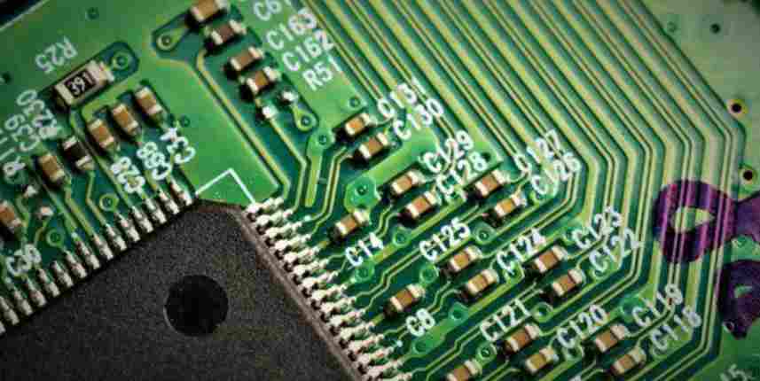


Just upload Gerber files, BOM files and design files, and the KINGFORD team will provide a complete quotation within 24h.