
Professional PCB manufacturing and assembly
Building 6, Zone 3, Yuekang Road,Bao'an District, Shenzhen, China
+86-13410863085Mon.-Sat.08:00-20:00

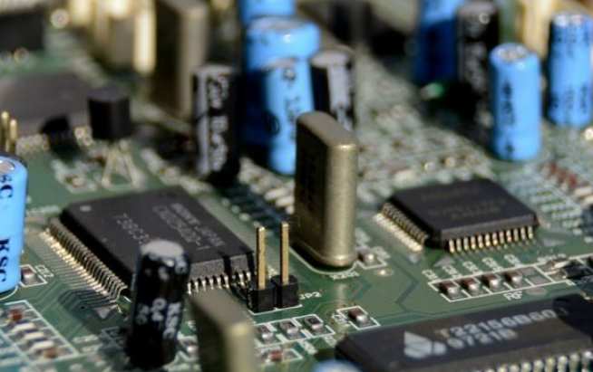
Coating alloying caused by uneven tin thickness is a common failure mode in hot air leveling (tin spraying) process of PCB. This article addresses this problem by sharing the following examples.
Bad analytic procedure
1. Visual inspection of appearance
Note: PCB padsurface treatment method is hot air leveling (spray tin).
2.EDS analysis
Note: There is no obvious solder paste (Sn) attached to the PAD of the failed solder joint, and no abnormal element is found, with C element accounting for about 30% (one of the main components of the flux).
3. Metallographic analysis of section
Description: Sectional analysis shows that the unwetted site is typical of surface alloying, i.e. exposed IMC layer.
4. SEM analysis of section
Note: The Sn thickness of PCB coating was analyzed, the section SEM of PAD position was analyzed, and the surface layer of PAD showed alloying state
Failure mechanism analysis
The uneven Sn coating thickness on the PCB surface leads to the alloying of the coating on the surface of the local welding pad, that is, the IMC layer (Cu6Sn5) is exposed. Because IMC contains a large amount of Cu, its melting point is much higher than that of the tin solder, which results in the reduction of the weldability of the surface of the welding pad, and the non-wetting of the welding pad and the solder climbing to the welding end of the device are easy to occur during reflow welding.
Allow me to begin this article in a traditional way by quoting the dictionary definition of "objective evidence" from a scientific point of view: "To be called science, an investigative method must follow specific principles of reasoning to collect observable, verifiable, and measurable evidence. The scientific method involves collecting data through observation and experimentation, and proposing and testing hypotheses." 1

Applying this definition to Chapter 8 of J-STD-001H (the "3 pages" mentioned in the title), we can see what needs to be done to meet the new requirements. Starting in 2020, J-STD-001 removes the industry-used ROSE test limit of 1.56μg/cm2nacl-equivalent ions or ionizable flux residues, which is a major concern for many companies.
This is understandable, given that the test has been the industry's only accepted standard measure of PCBA ion cleanliness since the 1970s. Think about that for a moment. When the standard was set in the 1970s, components were made with rosin flux containing about 35% solids and then cleaned with ozone-destroying chemicals. It was the era of gas-guzzling land yachts, power cars, bell-bottoms, platform shoes and sideburns. Those days are long gone, but while other electronic technology has changed, testing standards have not. Think about how much PCb, their components, and the way they are made have changed.
The industry has made great progress in processing capacity and miniaturization technology. But even though the industry has undergone such dramatic changes, acceptance criteria will not change until 2020. Of course, it can be said that even if the ROSE test limit is completely removed, the standard has not changed much.
Beyond that, we need to remember what the most important part of this whole discussion is: The ROSE test was never intended to be used to determine what qualifies as a manufacturing process. The idea is to use it only as a process monitoring tool during production to detect significant changes. Most assembly plants soon began using the ROSE test for process certification because, to be honest, it was not difficult to pass the test in most cases. Passing this test gives the impression that the processes used are trustworthy, that they meet established standards in the industry, and that everything is going smoothly, which may or may not be the case.
This is one of the major problems of using outdated acceptance criteria on highly technologically advanced components. What is the point of passing the test without concrete objective evidence that the process and materials are reliable? For decades, many manufacturers didn't think about this part. Contract manufacturers only manufacture products. In some cases, the cleanliness of their products is not enough to meet the requirements of the intended end-use environment. Typically, this defect manifests as a creepage related failure in the component shown in Figure 3, which has passed the ROSE test.
The component in Figure 3 uses a manual welding operation on the pins of the electroplated through-hole (PTH) connector. This process is the only one in the entire process that leaves a significant ionic residue, but no problem is detected as long as the average value of the entire surface area is used.
This would be a good time to bring up the topic of full board extraction with a focus area or local cleanliness analysis of sensitive parts -- but I digress. The point is that if the company had done more testing beforehand to determine what the ROSE results of the standard board should be, rather than blindly using 1.56g/cm2, it might have caught a small problem before it became a big one. All that said, let me just say that we can do better, and that's where the new J-STD-001H standard comes in.
Finding objective evidence to meet the requirements of the new standards is not as difficult to achieve as some might think. The underlying data may already exist in some form that meets the new requirements. I think this part of the process is overlooked by a lot of people, but it's there in black and white. Section 8.1 of J-STD-001H lists three methods for finding objective evidence. Note 2 mentions referring to historical evidence, review of returns, warranty service records, failure analysis results, etc., to show that the cause of failure is not related to cleanliness or ionic residue. This approach meets the standard without even having to do any new analysis. This method falls into the "if it ain't broke, don't fix it" category.
At no time has anyone empirically said that 1.56μg/cm2 is invalid for the product and process, only that this test can be demonstrated to indicate that the PCB has been cleaned. Note 3 says electrical testing of live products under conditions of high temperature and humidity using normal operating power supply. In my opinion, this is the most important test to determine the impact of ion cleanliness on field operations. Note 1 requires the assembly plant to perform a surface insulation resistance (SIR) analysis using some kind of test plate, most commonly IPC B-52CRET PCB, using a combination of equipment and materials used in the actual manufactured product, including bare plate solder mask, metallization, SMT solder paste flux, and flux for PTH welding. The aim is to mimic the end product as much as possible, to see if the product produced during assembly is not adversely affected when subjected to high temperatures and humidity. This test is often combined with ion chromatography analysis to determine the acceptable amount of residue after assembly. Once you have a mature process, you can also combine the ROSE test with SIR Analysis. If you plan to use ROSE testing to monitor the process flow, it is important to use your internal ROSE tester to determine what your acceptance criteria are.
SIR Is a new product acceptance requirement because obviously there is no historical evidence at that time. IPC-WP-019B is a great document that explains in detail how we can verify process reliability and, more importantly, what to do next. I confess at the outset that I was invited to contribute to the development of this document as a subject matter expert (SME), but can assure you that my contribution was negligible. I believe that the SME who actually contribute will agree with this. Honestly, this article could probably be boiled down to one sentence -- "For more details on cleanliness, refer to the WP-019B document." I don't know why I thought of it now, actually. It would have saved us all time.
WP-019B uses 28 pages to explain 3 pages of J-STD-001H, which strongly demonstrates the importance of cleanliness. In the WP-019 document, there are multiple examples of how objective evidence can be created, based on many instances of CM scale, and when a process process needs to be recertify for minor and major changes. In our lab, similar methods have been recommended for years.
If you plan to use ROSE to test and monitor the process flow, at least a cursory correlation study is required. I say rough correlation because there is no one-to-one comparison between ROSE and the IC test. The ROSE test measures the amount of soluble material throughout the process and provides resistivity measurements; The IC tells you exactly what the ion is and how many it is. You can make many sets of boards, a set of 50 (or some number that makes it easy to count), and then test 25 with IC and the remaining 25 with ROSE to see what the average is. If the average ROSE is lower than 1.56μg/cm2, the results are good. If it's higher than that, that's good. If there is historical data showing no contamination problems with the PCB, and the ROSE tester comes up with an average of 20 or 200µg/cm2, this is the number you need to use for that particular component.
This brings up another important issue: the need to certify each product separately due to differences in component architecture, density, and thermal mass. Each board has its own unique combination of parameters that can and likely will produce different results in the ROSE tester. So I say you should not use an empty reflow furnace to set the temperature curve when switching paste types. This is a good idea when calibrating and validating reflow furnaces, but when placing PCBS in reflow furnaces, the heat load should have an impact on the measurement of the finished components at critical locations. Just as the 1.56µg/cm2 cleanliness requirement does not apply to all components, it is also bad to validate reflow temperature curves with bare plates and then apply that temperature curve to all boards made with that solder paste. This is a bit off topic, but still important when trying to implement a qualified manufacturing process.
I fully believe that removing the 1.56µg /cm2 requirement over time will improve the overall quality and reliability of electronics as we have to look more carefully at the impact of residues on products manufactured today. I don't think it's as hard as some people think. I am confident that information on how to generate objective evidence is provided in Chapter 8 of J-STD-001H and WP-019B. As I have mentioned many times before, you are responsible for your own process quality and reliability, and the J-STD-001H standard can help the industry improve quality and reliability.
PCB fault after applying three anti paint
Feb 02,2023


Just upload Gerber files, BOM files and design files, and the KINGFORD team will provide a complete quotation within 24h.