
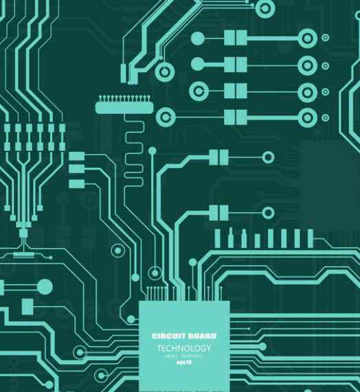
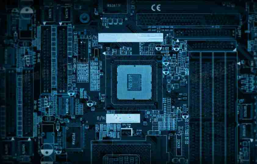
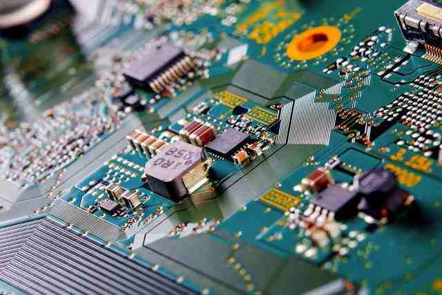
Professional PCB manufacturing and assembly
Building 6, Zone 3, Yuekang Road,Bao'an District, Shenzhen, China
+86-13410863085Mon.-Sat.08:00-20:00

I believe that most friends playing SMT process will first suspect whether it is solder paste printing (thickness, opening and pressure of steel mesh, etc.), over aging oxidation of solder paste, foot oxidation of SMD parts, or the temperature curve of reflow welding is not adjusted properly when they come across this SMD part.
The appearance of poor tin pcb is generally related to the cleanliness of PCB empty board surface. If there is no pollution, there will be no poor tin. Second, the solder itself is poor, temperature and so on.
Reasons for poor tin on PCB board:
1, the plate surface coating particle impurities, or the substrate in the process of manufacturing polishing particles left on the surface of the line.
2. The board is covered with grease, impurities and other sundries, or there is silicone oil residue
3. The plate surface has sheet electricity, and the plate surface coating has particle impurities.
4, the high potential coating is rough, there is a burning board phenomenon, the board surface has sheet electricity can not be tin.
5, the substrate or parts of the tin surface oxidation and copper surface dark situation is serious.
6, one side of the coating is complete, one side of the coating is bad, low potential hole side has obvious bright edge phenomenon.
7, low potential hole side has obvious bright edge phenomenon, high potential coating rough, there is burning plate phenomenon.
8. Insufficient temperature or time is not guaranteed in the welding process, or the flux is not used correctly
9, low potential large area can not be plated on tin, the board has a slight dark red or red, one side of the coating is complete, one side of the coating is bad.
Improvement and prevention of bad condition of electric tin on PCB board:
1. Periodic analysis of potion ingredients and timely addition, increase current density, prolong plating time.
2. Check the anode consumption from time to time and add the anode reasonably.
3. Cheerless tank analysis to adjust the content of light agent.
4. Reasonable adjustment of anode distribution, appropriate reduction of current density, reasonable design of board wiring or plate, adjust the light agent.
5. Strengthen ore-plating treatment.
6. Reduce the current density, and regularly maintain or treat the filtration system with weak electrolysis.
7. Strictly control the storage time and environmental conditions of the storage process, and strictly operate the production process.
8. Use solvent to clean sundries. If it is silicone oil, then it is necessary to use a special cleaning solvent to wash
9. Control PCB welding temperature at 55-80℃ and ensure sufficient preheating time
10. Use flux correctly.
The above is the "causes and improvement measures of defective tin on pcb board" compiled by Xiao bian. I hope it will be helpful to you. If you are not clear, please contact our customer service for your answer.
What documents need to be provided for pcb board production
After drawing the PCB board and checking all the details, we begin to select the PCB board factory. What work do we need to do after selecting the board factory?

PCB proofing is the early step of mass production, only accurate proofing can mass production, then, it is particularly important to provide accurate proofing documents, then everyone knows what documents need to be provided? And what should be noted in the documentation provided?
What documents should be provided for PCB board production?
1, first of all, you need to provide PCB or GERBER file, file to include plate making instructions, including the number of sub-layers of the board, material, pad process, ink color and other specific requirements, the following to understand the specific part of the main parameter description.
2. Materials: To explain what kind of materials are needed for PCB production, FR4 is the most common at present, and the main material is epoxy resin stripped fiber cloth board.
3. Board layer: The number of layers of PCB board should be explained. (The price of PCB board varies with the number of production layers, and the proofing process of PCB board is much the same)
4, welding resistance color: there are many kinds of color, can also be selected according to the requirements, the general is green.
5. Screen printing color: screen printing font and frame color on PCB, usually white.
6, copper thickness: generally according to the current of PCB circuit to scientifically calculate the thickness of copper, generally the thicker the better, but the cost will be higher, so the need for a reasonable balance.
7. Whether the hole is covered by welding resistance: welding resistance is to insulate the hole, otherwise it is not to insulate the hole.
8, surface coating: spray tin and gold plating, etc.
9. Quantity: The quantity of PCB should be clearly stated.


Just upload Gerber files, BOM files and design files, and the KINGFORD team will provide a complete quotation within 24h.