
Professional PCB manufacturing and assembly
Building 6, Zone 3, Yuekang Road,Bao'an District, Shenzhen, China
+86-13410863085Mon.-Sat.08:00-20:00

Diversification in materials, layers and processes to suit different electronic products and their special needs. The following summarizes some general differences, to briefly introduce the classification of PCB and its manufacturing method.
A. According to the material
a. Organic material
Phenolic resin, glass fiber /Epoxy resin, Polyimide, BT/Epoxy and other epoxy are among them.
b. Inorganic material
Aluminum, Copper-Invar-copper, ceramic and so on belong to it. Mainly for its heat dissipation function
B. The product is soft and hard
a. Rigid PCB
b. Flexible PCB
c. Rigid-Flex PCB
a. Single Panel (PCB)
b. Dual Panel (D-PCB)
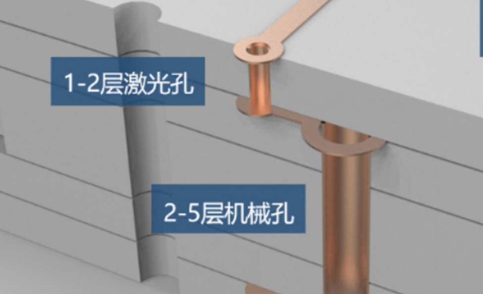
c. Multilayer board (PCB)
D. Divided by use: communication/consumable electronics/military/computer/semiconductor/electrical test board...
Another injection molding stereo PCB, due to less use, not introduced here.
Introduction of manufacturing method
A. Subtraction method,
B. Addition method, which can be divided into half addition and full addition method,
C. There are other advanced processes that have evolved in response to the evolution of IC packaging. This CD only mentions but does not cover them, as many are classified, not readily available, or not yet mature enough. This CD with the traditional negative multilayer board manufacturing process as the main axis, the introduction of each process in a simple way, and then supplemented by the concept of advanced technology to explore the future trend of PCB.
One, to be able to search
It is impossible to manufacture any number of PCBS without running into some problems, mainly due to the material of PCB choppered laminates. When quality problems occur in the actual manufacturing process, it also seems that PCB substrate materials are often the cause of the problem. Even a carefully written and executed technical specification for PCB laminates does not specify the tests that must be performed to determine that PCB laminates are the cause of manufacturing process problems. Here are some common PCB laminate problems and how to confirm them.

Once a PCB laminate problem is encountered, it should be considered to add to the PCB laminate material specification. Often, if this specification is not fleshed out, it will result in constant quality changes and consequent obsolescence. Usually, material problems arising from PCB laminate quality changes occur in products manufactured by manufacturers using different batches of materials or with different pressing loads. Few users maintain sufficient records to distinguish specific pressing loads or material batches at the processing site. As a result, PCBS are constantly produced and loaded with components and continuously warped in solder slots, wasting a lot of labor and expensive components. If the loading lot number is immediately available, the PCB laminate manufacturer can check the resin lot number, copper foil lot number, curing period, etc. That is, if the user does not provide continuity with the PCB laminate manufacturer's quality control system, the user himself suffers in the long run. The following describes the general issues related to substrate materials in the PCB manufacturing process.
Two, surface problems
Signs: poor print adhesion, poor coating adhesion, some parts can not be etched off, and some parts can not solder.
Possible inspection methods: Usually used for visual inspection by forming visible streaks of water on the surface of the plate:
Due to the very dense and smooth surface caused by the release film, the surface of the uncovered copper is too bright.
Usually on the copper-covered side of the laminate, the laminate manufacturer does not remove the release agent.
Pinholes in the copper foil cause the resin to flow out and accumulate on the surface of the copper foil, which is usually found on thinner copper foil than the 3/4 oz weight specification.
Copper foil makers apply excessive amounts of antioxidants to the surface of copper foil.
The laminate maker changed the resin system, the stripper, or the scrub method.
There are many fingerprints or greas,e stains due to improper operation.
Wet with oil during punching, blanking or drilling operations.
Possible solutions:
Laminate makers are advised to use fabric - like films or other release materials.
Contact the laminate manufacturer for mechanical or chemical removal.
Liaise with laminate manufacturer to inspect each batch of copper foil for non-conformity; Ask for a solution to remove the resin.
Ask the laminate maker for removal methods. General recommended the use of hydrochloric acid, followed by mechanical brush removal.
Cooperate with laminate manufacturer and specify user test items before any changes are made to laminate manufacture.
Teach all process personnel to wear gloves to handle copper-clad plates. Make sure that the laminate is shipped with the appropriate padding paper or in a bag, that the padding paper is low in sulfur, that the bag is free of dirt, and that no one touches the copper foil while using detergent containing silicone
Remove oil from all laminates prior to plating or graphic transfer process.


Just upload Gerber files, BOM files and design files, and the KINGFORD team will provide a complete quotation within 24h.