
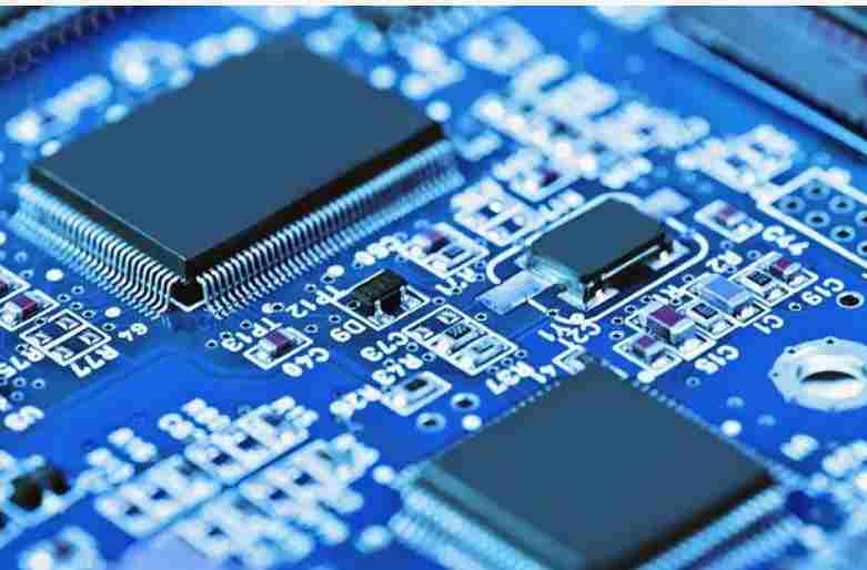
Professional PCB manufacturing and assembly
Building 6, Zone 3, Yuekang Road,Bao'an District, Shenzhen, China
+86-13410863085Mon.-Sat.08:00-20:00

PCBS have the following functions in electronic equipment.
(1) Provide mechanical support for fixing and assembling various electronic components such as integrated circuits, realize wiring and electrical connection or electrical insulation between various electronic components such as integrated circuits, and provide the required electrical characteristics.
(2) Provide solder resistance graphics for automatic welding, identification characters and graphics for component insertion, inspection and maintenance.
(3) Electronic equipment using printed board, because of the consistency of similar printed board, avoid manual wiring errors, and can realize the automatic insertion or installation of electronic components, automatic soldering, automatic detection, to ensure the quality of electronic products, improve labor productivity, reduce costs, and easy maintenance.
(4) Provide the electrical characteristics, characteristic impedance and EMC characteristics required for the circuit in high speed or high frequency circuits.
(5) Printed boards embedded with passive components provide certain electrical functions, simplify electronic installation procedures, and improve product reliability.
(6) It provides an effective chip carrier for miniaturized chip packaging of electronic components in large-scale and super-large-scale electronic packaging components.

Sort by layer
According to the circuit layer classification: divided into single panel, double panel and multi - layer board. The common multilayer board is generally 4 layers or 6 layers, complex multilayer board can reach dozens of layers. There are three main types of PCB boards:
Single panel
Single-Sided Boards On most basic PCBS, parts are concentrated on one side and wires on the other (with patch components on the same side as wires and add-ons on the other side). Because wires appear on only one side, this type of PCB is called Single-sided. Only early circuits used such boards because a single panel had many severe limitations on the design circuit (because there was only one side, the wiring could not be crossed and had to be routed in a separate path).
Dual panel Dual panel
Double-Sided Boards have wiring on both sides, but to use wire on both sides, there must be proper circuit connections between them. This "bridge" between circuits is called a pilot hole (via). A pilot hole is a small hole in a PCB filled with or coated with metal that can be connected to wires on both sides. Because the area of the dual panel is twice as large as that of the single panel, the dual panel solves the difficulty of the single panel due to the interleaving of the wiring (can be routed to the other side through the hole), and it is more suitable for the more complex circuit than the single panel.
Multilayer board
To increase the area that can be wired, Multi-Layer Boards use more single or double-sided wiring boards. A printed circuit board with a double-sided inner layer, two single-sided outer layer or two double-sided inner layer, two single-sided outer printed circuit board, through the positioning system and insulating binder materials alternately together and conductive graphics in accordance with the design requirements of the interconnection of the printed circuit board becomes a four-layer, six-layer printed circuit board, also known as the multilayer printed circuit board. The number of layers of the board does not mean that there are several independent wiring layers. In special cases, empty layers will be added to control the thickness of the board. Usually, the number of layers is even and includes the outermost two layers. Most of the main board is 4 to 8 layers of structure, but technically theory can be done close to 100 layers of PCB board. Most large supercomputers use quite a few layers of mainframe boards, but because such machines can be replaced by clusters of ordinary computers, super-multiboards have fallen out of use. Because the layers in the PCB are so tightly integrated, it is not always easy to see the actual number, but if you look closely at the main board, you can see it.
Categorize by hard and soft
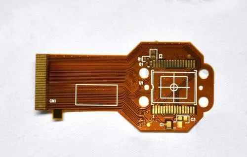
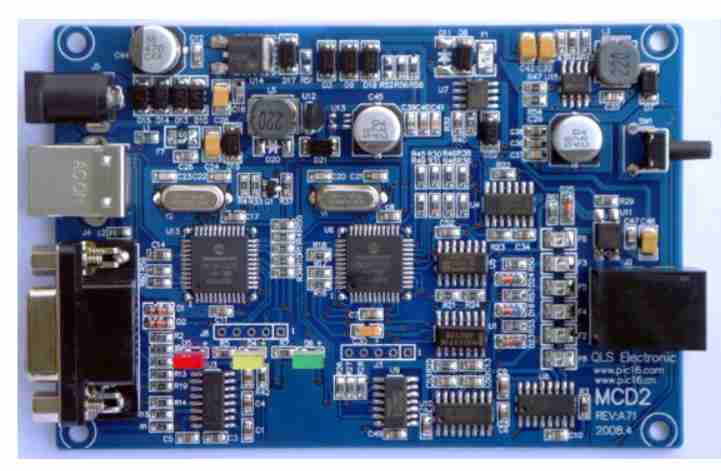
Divided into rigid circuit board and flexible circuit board, soft and hard combined board. Generally, Rigid PCB shown in the first figure below is called rigid PCB, and the yellow connection wires in the second figure are called Flexible (or Flexible)PCB. The intuitive difference between rigid and flexible PCBS is that flexible PCBS can be bent. The common thickness of rigid PCB is 0.2mm, 0.4mm, 0.6mm, 0.8mm, 1.0mm, 1.2mm, 1.6mm, 2.0mm, etc. The common thickness of flexible PCB is 0.2mm, where the parts to be welded will be added to the back of the thickened layer, the thickness of the thickened layer is 0.2mm,0.4mm. The purpose of understanding this is to provide structural engineers with a spatial reference when designing. Common rigid PCB materials include: phenolic paper laminate, epoxy paper laminate, polyester glass felt laminate, epoxy glass cloth laminate; Flexible PCB materials commonly include: polyester film, polyimide film, fluoride ethylene propylene film.
PCB design principles
To obtain the best performance of electronic circuits, component layout and wire layout are very important. In order to design good quality, low cost PCB. The following general principles should be followed:
layout
First, consider the PCB size. PCB size is too large, printing line is long, impedance increases, anti-noise ability decreases, the cost also increases; Too small, the heat dissipation is not good, and the adjacent lines are susceptible to interference. After the PCB size is determined, the location of special components is determined. Finally, according to the functional unit of the circuit, the layout of all components of the circuit.
The following principles should be observed when determining the location of special components:
(1) Shorten the connection between high-frequency components as far as possible, and try to reduce their distribution parameters and electromagnetic interference between each other. Easily disturbed components should not be too close to each other, input and output components should be as far away as possible.
② There may be a higher potential difference between some components or wires. The distance between them should be increased to avoid accidental short circuit from discharge. Components with high voltage should be arranged as far as possible in places that are not easily touched by the hand during debugging.
(3) Components weighing more than 15 g should be fixed with a support, and then welded. Those large and heavy, heat components, should not be installed on the printed board, but should be installed on the chassis bottom, and should consider the problem of heat dissipation. The heat sensitive element should be far away from the heating element.
④ The layout of adjustable components such as potentiometer, adjustable inductor coil, variable capacitor, micro switch should consider the structural requirements of the whole machine. If the machine adjustment, should be placed above the printed board for easy to adjust the place; If the outside of the machine adjustment, its position to adjust the knob on the chassis panel position.
According to the functional unit of the circuit, the layout of all components of the circuit should comply with the following principles:
(1) Arrange the position of each functional circuit unit according to the flow of the circuit, so that the layout is convenient for signal flow, and make the signal as consistent as possible.


Just upload Gerber files, BOM files and design files, and the KINGFORD team will provide a complete quotation within 24h.