
Professional PCB manufacturing and assembly
Building 6, Zone 3, Yuekang Road,Bao'an District, Shenzhen, China
+86-13410863085Mon.-Sat.08:00-20:00

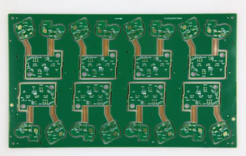
Cause of Copper Exposed in Hot Air Leveling Process of Soft and Hard Bonded Plate
What are the reasons for the exposure of copper in the hot air leveling process of soft and hard composite boards explained to you by PCB manufacturers, PCB designers and PCBA processors?
Hot air leveling is to immerse the printed circuit board into the molten solder, and then blow off the excess solder on its surface and in the metallized hole with hot air to obtain a smooth, uniform and bright solder coating with good solderability and no exposed copper. Copper exposed on the pad surface and in the metallized hole after hot air leveling is an important defect in the finished product inspection, which is one of the common reasons for hot air leveling rework. Then, what are the reasons for the hot air leveling of the soft and hard bonding plates? Come and have a look with Xiao Bian~
The pre-treatment is insufficient and the coarsening is poor. The quality of the hot air leveling pretreatment process has a great impact on the quality of the hot air leveling. In this process, the oil, impurities and oxide layer on the bonding pad must be completely removed to provide a fresh solderable copper surface for tin dipping. Mechanical spraying is a common pretreatment process. Copper exposure caused by poor pre-treatment occurs in large numbers, and copper exposure points are often distributed throughout the board, especially on the edges. In case of similar situations, chemical analysis shall be carried out for the micro etching solution, the second pickling solution shall be checked, the concentration of the solution shall be adjusted, and the solution that is seriously polluted due to too long use time shall be replaced, and the spraying system shall be checked for smoothness. Proper extension of treatment time can also improve the treatment effect.
2. The pad surface is not clean, and there is residual solder resistance polluting the pad. Most manufacturers use full screen printing liquid photosensitive solder mask ink, and then remove the excess solder mask through exposure and development to obtain the solder mask of time. Whether there are defects on the solder mask, whether the composition and temperature of the developing solution are correct, and whether the developing speed, i.e. the developing point, is correct. Any of these conditions will leave a residue on the pad. In general, a post shall be set up before the curing process for the design of soft and hard bonding plates to inspect the interior of graphics and metallized holes to ensure that the bonding pads and metallized holes of printed circuit boards sent to the next process are clean and free of solder blocking ink residues.
3. Insufficient activity of flux. The role of the flux is to improve the wettability of the copper surface, protect the laminate surface from overheating, and provide protection for the solder coating. If the activity of the flux is not enough and the wettability of the copper surface is not good, the solder cannot completely cover the pad, and the copper exposure is similar to the poor pre-treatment. Prolonging the pre-treatment time can reduce the copper exposure. The selection of a stable and reliable flux by the process technician has an important impact on the hot air leveling, and the excellent flux is the guarantee of the hot air leveling quality.
The above is the cause analysis of copper exposure in the hot air leveling process of soft and hard bonding plates. Do you understand it? What are the reasons for the exposure of copper in the hot air leveling process of soft and hard composite boards explained to you by PCB manufacturers, PCB designers and PCBA processors?


Just upload Gerber files, BOM files and design files, and the KINGFORD team will provide a complete quotation within 24h.