
Professional PCB manufacturing and assembly
Building 6, Zone 3, Yuekang Road,Bao'an District, Shenzhen, China
+86-13410863085Mon.-Sat.08:00-20:00

Difficulties in Multilayer Circuit Board Processing and Flexible Circuit Board Welding
The circuit board manufacturing, circuit board design and PCBA processing manufacturers explain the four difficulties in multi-layer circuit board processing and how to deal with the poor soldering of flexible circuit boards
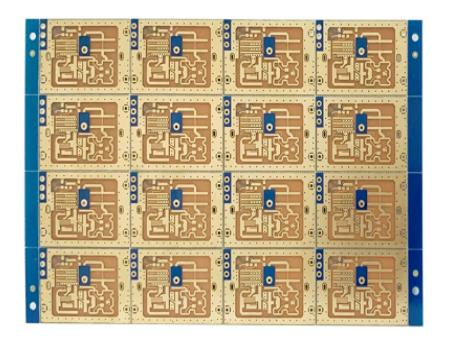
What are the four major difficulties in the production and processing of multilayer circuit boards?
1. Difficulties in making inner line
Multi layer circuit of circuit board has various special requirements for high speed, thick copper, high frequency and high Tg value, and the requirements for inner layer wiring and graphic size control are getting higher and higher. For example, there are many impedance signal lines in the inner layer of the ARM development board. To ensure the integrity of the impedance increases the difficulty of the inner layer circuit production.
There are many signal lines in the inner layer, and the width and spacing of lines are basically about 4mil or less; It is easy to wrinkle in the production of thin multi-core board, which will increase the production cost of the inner layer.
2. Difficulties in alignment between inner layers
With more and more layers of circuit boards, the alignment requirements of the inner layers are also getting higher and higher. Film will expand and shrink due to the influence of workshop environment temperature and humidity, and the core board will expand and shrink the same after production, which makes the alignment accuracy between inner layers more difficult to control.
3. Difficulties in pressing process
The superposition of multiple core plates and PP (prepreg) is prone to delamination, slide plate and steam drum residue during pressing. The number of layers is large, and the control of expansion and contraction and the compensation of size coefficient cannot keep consistent; The thin interlayer insulation layer is easy to lead to the failure of interlayer reliability test.
4. Difficulties in drilling production
High Tg or other special plates are used for multilayer boards of circuit boards. The roughness of drilling holes made of different materials is different, which increases the difficulty of removing the glue residue in the holes. The high-density multilayer board has high hole density, low production efficiency, and is easy to break the tool. The hole edge between holes of different networks is too close, which will lead to the CAF effect problem.
Therefore, in order to ensure the high reliability of the final product, the circuit board manufacturer needs to carry out corresponding control during the production process
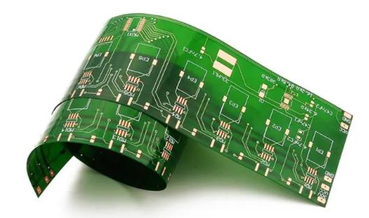
How to deal with poor welding of FPC? You should know these methods
In the process of FPC chip processing, we often encounter some electronic components with poor welding. In the face of such electronic components, we will generally remove the electronic components with incorrect welding without damaging the FPC board. So today, the FPC factory will introduce the method of removing and welding the FPC chip.
Dismantle welding method:
(1) Split point desoldering method: for resistance capacitance components installed horizontally, the two welding points are far away, so electric soldering iron can be used for split point heating and point by point extraction. If the pin is bent, pry it with a soldering iron head and then remove it. During desoldering, erect the fpc, heat the pin solder joints of the components to be disassembled with an electric soldering iron, and gently pull out the component pins with tweezers or pointed nose pliers.
(2) Centralized desoldering method: since each pin of the row resistor is welded separately, it is difficult to heat it at the same time with an electric soldering iron. You can use a hot air welder to quickly heat several welding points, and pull them out once after the solder melts.
(3) Preserve the desoldering method: first, use the tin absorbing tool to absorb the solder of the desoldered joint. Generally, components can be removed. In case of multi pin electronic components, the electronic hot air fan can be used for heating.
If the components or pins are overlapped, the solder joint can be dipped with flux, the solder joint can be opened with an electric soldering iron, and the pins or wires of the components can be removed. If it is a hook welded component or pin, first remove the solder from the solder joint with an electric soldering iron, and then heat it with an electric soldering iron to melt the residual solder under the hook. At the same time, use a blade to lift the pin in the direction of the hook. Do not use excessive force when prying to prevent molten solder from splashing into eyes or clothes.
(4) Cutting and desoldering method: if there is any margin in the component pins and wires on the removed solder joints, or if it is determined that the components are damaged, the components or wires can be cut off first, and then the wire ends on the bonding pad can be removed. The circuit board manufacturing, circuit board design and PCBA processing manufacturers will explain to you how to deal with the four difficulties in multi-layer circuit board processing and the poor soldering of flexible circuit boards.


Just upload Gerber files, BOM files and design files, and the KINGFORD team will provide a complete quotation within 24h.