
Professional PCB manufacturing and assembly
Building 6, Zone 3, Yuekang Road,Bao'an District, Shenzhen, China
+86-13410863085Mon.-Sat.08:00-20:00

Detailed explanation of PCB circuit and resistance welding process
PCB manufacturing, PCB design and PCBA processing manufacturers will explain PCB circuit and solder mask process in detail
The design of printed circuit board is based on the circuit schematic diagram to realize the functions required by the circuit designer. The design of printed circuit board mainly refers to layout design, which needs to consider the layout of external connections. The optimal layout of internal electronic components, the optimal layout of metal wiring and through-hole, electromagnetic protection, heat dissipation and other factors. Excellent layout design can save production costs and achieve good circuit performance and heat dissipation. Simple layout design can be realized by hand, while complex layout design needs to be realized by computer aided design (CAD)
As we all know, in the process of PCB printing, the circuit and solder mask technology, as an important part, have made outstanding contributions to the board's "beautiful coat"! How is the resistance welding process subdivided?
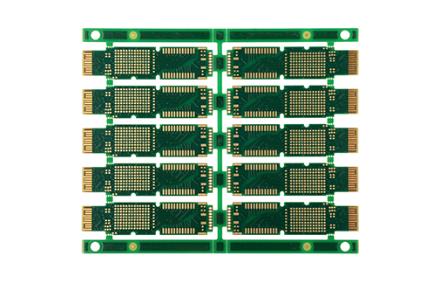
Because the common ink color of PCB is green, accounting for more than 90% of the PCB industry, solder mask is also called green oil,
Solder resist inks can be divided into photosensitive inks and non photosensitive inks according to their photosensitive properties. Photosensitive inks are commonly used.
When the outer layer of lines is formed on the board surface through the line process, a layer of "protective film" shall be formed through the resistance welding process, which aims to expose the holes to be welded on the board surface, and provide a long-term insulation environment in other places to prevent short circuit, etc.
The general processes of solder mask process can be divided into: green oil washing, pretreatment, silk screen green oil, pre baking, alignment/exposure, development, QC inspection, plate receiving, curing and post process.
To put it simply, after removing the oxides and impurities on the PCB surface, roughening the copper surface and enhancing the adhesion of the green oil on the PCB surface, we apply the green oil for printing by silk screen or coating, then harden the green oil by pre baking, expose the copper surface by exposure, and finally develop the board as required by the customer.
In the process, we can divide solder mask printing into silk screen process and coating process. The silk screen process is a conventional solder mask ink covering method, which is used to make products with high appearance requirements and can meet the appearance inspection standards of IPCI level and above.
The coating process is an efficient solder mask ink covering method. The ink thickness can meet the conventional requirements, but there will be slight oil accumulation at the edge of the large hole. The products made by this method have general appearance requirements, and the appearance quality requirements meet the appearance inspection standards of IPC Class I and below. Resistance welding also has different imaging methods in different boards. For example, double-sided and multi-layer boards only have exposure resistance welding. Single panel and aluminum substrate have exposure, thermosetting and UV resistance welding~
If you want the board to be both beautiful and practical, green materials, process accuracy and equipment are very important! PCB manufacturing, PCB design and PCBA processing manufacturers will explain PCB circuit and solder mask process in detail.


Just upload Gerber files, BOM files and design files, and the KINGFORD team will provide a complete quotation within 24h.