
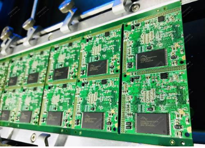
Professional PCB manufacturing and assembly
Building 6, Zone 3, Yuekang Road,Bao'an District, Shenzhen, China
+86-13410863085Mon.-Sat.08:00-20:00

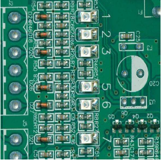
The full name of BGA is Ball Grid Array (PCB with ball grid array structure), which is a packaging method using organic carrier plates for integrated circuits. It has the following characteristics: ① the package area is reduced; ② the function is increased; the number of pins is increased; ③ the PCB board can be self centered when soldering; ④ it is easy to tin; ④ the reliability is high; ⑤ the electrical performance is good; and the overall cost is low. PCB boards with BGA generally have many small holes. Most customers' BGA lower vias are designed with a finished hole diameter of 8~12 mil. The distance from the surface of the BGA to the hole is 31.5 mil, for example, which is generally not less than 10.5 mil. The lower vias of the BGA need to be plugged, the BGA pad is not allowed to be inked, and the BGA pad is not allowed to be drilled.
At present, our company mainly adopts the following processes for the BGA lower via plug hole: ① Flat the front plug hole: it is applicable to the BGA plug hole where the resistance welding is exposed on one side or partially. If the difference between the two plug hole diameters is 1.5mm, this process is adopted regardless of whether the resistance welding is covered on both sides; ② Solder resistance plug hole: used for welding the plate covered on both sides at the BGA plug hole; ③ Plug hole before and after leveling: used for thick copper foil or other plates with special needs. There are 7 kinds of plug drilling sizes: 0.25, 0.30, 0.35, 0.40, 0.45, 0.50 and 0.55mm.
What should BGA do in CAM production?
1、 Fabrication at outer line BGA:
Before processing the customer's data, we should fully understand the specification of BGA, the size of the pad designed by the customer, the array, the size of the via under BGA, the distance from the hole to the BGA pad, and PCB boards with a copper thickness of 1~1.5 ounces. Except that the production of specific customers should be compensated according to their acceptance requirements, other customers should generally compensate for 2 mils if they use the mask etching process in production, and 2.5 mils if they use the graphic technology, The specification of 31.5mil BGA is not processed by graphic electric process; When the distance between BGA and vias designed by customers is less than 8.5mil, and the lower vias of BGA are not centered, the following methods can be used:
A standard BGA array can be made according to the BGA specification and design pad size corresponding to the BGA position designed by the customer, and then the BGA and BGA lower vias to be corrected can be photographed based on the BGA specification and design pad size. After being photographed, the effect before and after the snapshot should be checked by comparing with the original backup level before the snapshot. If the BGA pad has a large deviation before and after the snapshot, it cannot be used, and only the position of BGA lower vias should be photographed.
2、 BGA resistance welding production:
1. BGA surface mount solder mask opening: as the solder mask optimization value, the single side opening range is 1.25~3mil, and the distance between solder mask lines (or via pads) is no less than 1.5ml;
2. Treatment of BGA plug hole template layer and base plate layer:
① Make 2MM layer: copy the BGA pad of the circuit layer as another layer of 2MM layer and treat it as a square in the range of 2MM. No blank or gap is allowed in the middle of 2MM (if the customer requires that the character box at BGA be used as the plug hole range, the character box at BGA be used as the 2MM range for the same treatment). After the 2MM entity is made, compare it with the character box at BGA of the character layer, and the larger one is the 2MM layer.
② Plug hole layer (JOB. bga): touch the 2MM layer with the hole layer (select from the 2MM layer with the Actions à reference selection function in the panel), select Touch for the parameter Mode, copy the holes to be plugged within the BGA 2MM range to the plug hole layer, and name it JOB Bga.
③ Copy the plug hole layer as another base plate layer (JOB. sdb).
④ Adjust the hole diameter of the plug hole layer and the hole diameter of the base plate layer according to the BGA plug hole file.
3、 Processing of BGA corresponding hole blocking layer and character layer:
① Where the hole plugging is required, there is no stop point on both sides of the hole plugging layer;
② The white oil is allowed to enter the hole where the character layer is opposite to the plug hole.
After the above steps are completed, the board production of BGA CAM is completed. This is just the current situation of the board production of BGA CAM. In fact, due to the rapid change of electronic information products and the fierce competition in the PCB industry, the production procedures for BGA plug holes are often replaced, and new breakthroughs are constantly emerging. Each breakthrough makes the product go to a higher level and adapt to the changing requirements of PCB market. We look forward to more superior BGA plug hole or other processes.


Just upload Gerber files, BOM files and design files, and the KINGFORD team will provide a complete quotation within 24h.