
Professional PCB manufacturing and assembly
Building 6, Zone 3, Yuekang Road,Bao'an District, Shenzhen, China
+86-13410863085Mon.-Sat.08:00-20:00

Pcb manufacturer explains the near hole problem of rogers circuit board
PCB manufacturers, PCB designers and PCBA manufacturers explain to you the PCB manufacturers about the near hole problem of Rogers PCB
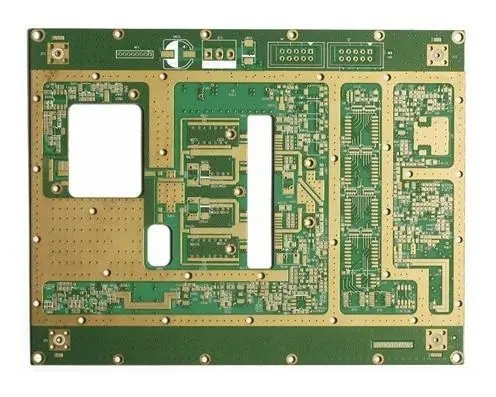
Rogers PCB high-frequency board factories often encounter the problem that "the hole to line is too close, which exceeds the process capability". When we design Rogers PCB high-frequency board, we mostly consider how to connect the layers with the network signal lines in the most reasonable way. The denser the lines on Rogers PCB are, the denser the vias (VIA) will be, and the vias can play the role of electrical connection between layers.
Then, what kind of difficulties will the near hole cause to the production? What near hole problems should we pay attention to?
If two holes are too close to each other during drilling operation, the efficiency of PCB drilling process will be affected. After the first hole is drilled, the material on one side will be too thin when drilling the second hole, which will lead to uneven stress on the drill bit and uneven heat dissipation of the drill bit, resulting in broken drill bit, which will cause the hole collapse of Rogers circuit board or incomplete drilling.
2. The vias in Rogers circuit board will have hole rings on each layer of circuit, and the surrounding environment of each layer of hole ring is different, with or without wire clamping. When optimizing documents, the CAM engineer of the PCB factory will cut off a part of the hole ring when the wire clamp is too close or the hole is too close to the hole, so as to ensure that there is a safe distance of 3mil between the welding ring and different network copper/wire.
3. The hole position tolerance of drilling is ≤ 0.05mm. When the tolerance goes to the upper limit, the following situations will occur in Rogers circuit board multilayer board:
(1) When the lines are dense, small gaps occur irregularly 360 ° from vias to other elements. To ensure a safe distance of 3mil, the pad may be cut in multiple directions.
(2) According to the calculation of source file data, 6mil from hole edge to line edge, 4mil from hole ring, and 2mil from ring to line. To ensure a safety distance of 3mil from ring to line, 1mil welding ring needs to be cut, and only 3mil for pad after cutting. When the tolerance deviation of hole position is 0.05mm (2mil), there is only 1mil left for the hole ring.
4. Rogers circuit board production will have a small amount of offset in the same direction, and the pad will be cut in an irregular direction. In the worst case, individual holes will be damaged.
5. The influence of pressing deviation of Rogers circuit board inner layer. Take a six ply board as an example, three core boards+copper foil are laminated to form a six ply board. During pressing, core plate 1, core plate 2 and core plate 3 may have a deviation of ≤ 0.05mm during pressing, and the inner layer hole will also have an irregular deviation of 360 ° after pressing.
From the above problems, it can be concluded that the yield of Rogers circuit board proofing and the production efficiency of PCB high-frequency board are affected by the drilling process. If the hole ring is too small and there is no complete copper sheet protection around the hole, although the PCB can pass the open and short circuit test and there will be no problems in the early use of the product, the long-term use reliability is still insufficient.
Therefore, suggestions on hole to hole and hole to wire spacing of Rogers circuit board and high-frequency board are given:
(1) Rogers circuit board multi-layer inner layer hole to wire to copper:
4th floor: no pipe
6 layers: ≥ 6mil
8th floor: ≥ 7mil
10 layers or more: ≥ 8mil
(2) Clearance between inner diameter edges of vias:
Same network via: ≥ 8mil (0.2mm)
Via of different networks: ≥ 12mil (0.3mm)
PCB manufacturers, PCB designers and PCBA manufacturers will explain to you the PCB manufacturers about the near hole problem of Rogers PCB.


Just upload Gerber files, BOM files and design files, and the KINGFORD team will provide a complete quotation within 24h.