
Professional PCB manufacturing and assembly
Building 6, Zone 3, Yuekang Road,Bao'an District, Shenzhen, China
+86-13410863085Mon.-Sat.08:00-20:00

Solve the welding method of double-sided circuit board in one paper
Circuit board manufacturing, circuit board design and PCBA processing manufacturers explain how to solve the welding method of double-sided circuit boards
01 - PCB welding skills
Soldering skill 1:
The process flow of selective welding includes: flux spraying, circuit board preheating, dip welding and drag welding. Flux coating process plays an important role in selective welding.
When welding heating and welding is completed, the flux shall have enough activity to prevent bridging and oxidation of the circuit board. Flux spraying The X/Y manipulator carries the circuit board over the flux nozzle, and the flux is sprayed to the soldering position of the pcb circuit board.
Soldering circuit board skill 2:
For the microwave peak selection welding after the reflow welding sequence, it is important to spray the flux accurately, and the micro hole spray type will not contaminate the area outside the solder joint.
The diameter of the spot pattern of micro spot spraying flux is greater than 2mm, so the position accuracy of the flux sprayed and deposited on the circuit board is ± 0.5mm to ensure that the flux always covers the part to be welded.
Soldering skill 3:
The process characteristics of selective welding can be understood by comparing with wave soldering. The obvious difference between the two is that the lower part of the circuit board in wave soldering is completely immersed in liquid solder, while in selective soldering, some specific areas are in contact with solder waves.
As the circuit board itself is a bad heat conduction medium, it will not heat and melt the solder joints of adjacent components and circuit board areas during welding.
Before welding, the flux must also be coated in advance. Compared with wave soldering, the flux is coated on the lower part of the circuit board to be welded, rather than the entire pcb circuit board.
In addition, selective welding is applicable to the welding of plug-in components. Selective welding is a new method. A thorough understanding of the selective welding process and equipment is necessary for successful welding.
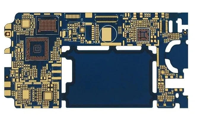
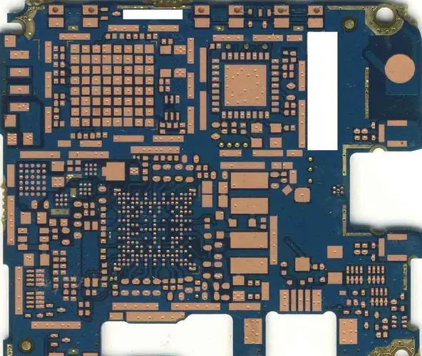
picture
02 - Precautions for PCB welding
Remind everyone that after getting the bare PCB board, they should first conduct appearance inspection to see if there are short circuit, open circuit and other problems, and then get familiar with the schematic diagram of the development board, compare the schematic diagram with the PCB screen layer, to avoid inconsistency between the schematic diagram and PCB.
After the materials required for PCB welding are fully prepared, the components shall be classified. All components can be divided into several categories according to size for subsequent welding. A complete material list shall be printed. In the process of welding, if one item has not been welded, the corresponding option shall be crossed off with a pen to facilitate subsequent welding operations.
Before welding, anti-static measures such as wearing electrostatic rings should be taken to avoid damage to components caused by static electricity. After the equipment required for welding is fully prepared, the welding head shall be kept clean and tidy. It is recommended to use a flat angle soldering iron for initial welding. The soldering iron can better contact the bonding pad when welding components such as 0603 package, which is convenient for welding. Of course, this is not a problem for experts.
When selecting components for welding, the welding shall be carried out according to the sequence of components from low to high and from small to large. In order to avoid inconvenience to the welding of smaller components due to large components welded well. Soldering of integrated circuit chips is preferred.
Before welding the integrated circuit chip, ensure that the chip is placed in the correct direction. For the chip screen layer, generally the rectangular pad represents the starting pin. During welding, a pin of the chip shall be fixed first, and the position of the components shall be fine adjusted, then the diagonal pin of the chip shall be fixed, so that the components can be accurately connected to the position before welding.
There is no difference between positive and negative electrodes for zener diodes in chip ceramic capacitors and voltage stabilizing circuits, while positive and negative electrodes need to be distinguished for light-emitting diodes, tantalum capacitors and electrolytic capacitors. For capacitor and diode components, the end with obvious mark shall be negative. In the chip mounted LED package, the direction along the lamp is positive negative. For the components and parts packaged with diode circuit diagram marked by silk screen, the negative terminal of diode shall be placed at the end with vertical line.
For crystal oscillators, passive crystal oscillators generally have only two pins, and there is no difference between positive and negative. The active crystal oscillator generally has four pins, so pay attention to the definition of each pin to avoid welding errors.
For the welding of plug-in components, such as power module related components, the device pins can be modified before welding. After the components are placed and fixed, the soldering tin is generally melted on the back by soldering iron and then integrated into the front by the bonding pad. Solder does not need to be put too much, but the components should be stabilized first.
During welding, PCB design problems found shall be recorded in time, such as installation interference, incorrect pad size design, component packaging error, etc., for future improvement.
After welding, use a magnifying glass to check the welding spot to see if there is any false welding or short circuit.
After the welding of the circuit board is completed, the circuit board surface shall be cleaned with alcohol and other cleaning agents to prevent the circuit from being short circuited by iron filings attached to the circuit board surface, which can also make the circuit board cleaner and more beautiful.
03 - Characteristics of double-sided circuit board
The difference between single-sided circuit boards and double-sided circuit boards is the number of copper layers. Science popularization: The double-sided circuit board has copper on both sides of the circuit board, which can be connected through the via. The single side has only one layer of copper, which can only be used for simple circuits, and the holes can only be used for plug-ins, which cannot be connected.
The technical requirements of double-sided circuit boards are that the wiring density becomes larger, the aperture is smaller, and the aperture of metallized holes is smaller and smaller. The quality of the metallized holes on which the interconnection between layers depends is directly related to the reliability of printed boards.
With the reduction of the hole diameter, the impurities that have no effect on the larger hole diameter, such as grinding and brushing debris and volcanic ash, once left in the small hole, will make the chemical copper deposition and electroplating copper ineffective, and the hole will be free of copper, which is fatal to the hole metallization.
04 - Welding method of double-sided circuit board
In order to ensure reliable conductive effect of double-sided circuit board, it is recommended that the connection holes (i.e. metallization process through-hole part) on the double-sided circuit board should be welded with wires and the like, and the protruding part of the connection wire tip should be cut off to avoid hurting the operator's hand. This is the preparation for connecting the board.
Key points of double-sided circuit board welding:
Components requiring reshaping shall be processed according to the requirements of the process drawing; That is, plastic before plug-in
After reshaping, the model surface of diode shall be upward, and the length of two pins shall not be inconsistent.
When inserting the components with polarity requirements, it shall be noted that the polarity shall not be reversed. After the roll integrated block components are inserted, no vertical or horizontal components shall have obvious inclination.
The power of the electric soldering iron used for welding is 25~40W. The temperature of the electric soldering iron head should be controlled at about 242 ℃. If the temperature is too high, the head is easy to "die". If the temperature is too low, the solder cannot be melted. The welding time should be controlled at 3~4s.
Formal welding is generally carried out according to the principle of welding components from low to high and from inside to outside. The welding time should be well controlled. If the welding time is too long, the components will be damaged and the copper clad strip on the copper clad plate will also be damaged.
Because it is double-sided welding, a process frame for placing the circuit board and the like should also be made, so as not to squint the devices below.
After the welding of the circuit board is completed, it is necessary to carry out a number based inspection in many aspects, check the places where there is missing insertion and welding, trim the redundant device pins of the circuit board after confirmation, and then flow to the next process.
In the specific operation, the relevant process standards shall be strictly followed to ensure the welding quality of products.
With the rapid development of high-tech, electronic products closely related to the public are constantly updated. The public also needs electronic products with high performance, small size and multiple functions, which puts forward new requirements for circuit boards. This is why double-sided circuit board was born. Due to the wide application of double-sided circuit board, the manufacturing of printed circuit board is also developing towards light, thin, short and small.
Circuit board manufacturing, circuit board design, PCBA processing manufacturers will explain the method of double-sided circuit board welding.


Just upload Gerber files, BOM files and design files, and the KINGFORD team will provide a complete quotation within 24h.