
Professional PCB manufacturing and assembly
Building 6, Zone 3, Yuekang Road,Bao'an District, Shenzhen, China
+86-13410863085Mon.-Sat.08:00-20:00

Analysis of Three Kinds of PCB Ink and the Naming of PCB
The circuit board manufacturer, circuit board designer and PCBA manufacturer will explain the three types of circuit board ink and the naming method of circuit board
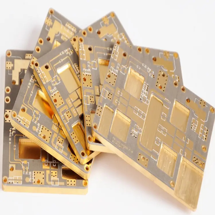
Those who are familiar with PCB know that PCB needs ink. At present, there are many kinds of ink on the market. PCB ink is mainly divided into three categories: circuit ink, solder resist ink and character ink.
1. Line ink
As a barrier layer to prevent corrosion of the circuit, it protects the circuit during etching. It is generally liquid photosensitive. There are two kinds of acid corrosion resistance and alkali corrosion resistance. Alkali resistance is more expensive. This layer of ink should be dissolved with alkali after it is corroded out of the circuit.
2. Solder resist ink
It is painted on the line after the line is completed to protect the line. There are liquid photosensitive, heat cured, and ultraviolet hardened ones. The bonding pad is reserved on the board, which is convenient for soldering components and plays the role of insulation and oxidation prevention.
3. Character ink
It is used to mark the surface of the board, such as component symbols, and it is generally white.
In fact, there are other inks, such as peelable ink, which can be removed after protecting the parts that do not need to be treated during copper plating or surface treatment; Silver paste ink and so on. These are the general types of PCB ink.
What is the naming method of PCB design circuit board?
There are many kinds of PCBs. Different kinds have different naming methods. Here we introduce the naming methods of common PCBs.
1. Through hole pad
Naming format: THC (R, O) 90x60d40x20.
Note: THC stands for through hole round hole, THR stands for rectangular pad (square is the same in length and width), and THO stands for oval pad.
90x60 represents a length of 90mil and a width of 60mil. If it is a circle, just write a number.
D40x20 represents a hole with an inner diameter of 40mil long and 20mil wide. The original headline today is Wolong Club IT technology.
The other is THC (O) N, followed by an N (that is, NTH), which represents a nonmetallic hole pad.
2. Surface mount pad
Naming format: SMDC (R, O) 90x60
Note: This command has similarities and differences with the above through hole pad command. C stands for circle, for example, MARK point is circular, R stands for rectangle, which is the most, and O stands for ellipse.
The rear 90x60 is the length and width.
These surface mounted components generally refer to the pads on the front side. Generally, the front side is used as the common component surface for packaging. If there are special ones that need to be placed on the reverse side when packaging, then add a_ b. For example, SMDC90X60_ b. Represents a pad placed on the opposite side.
3. Through-hole
Naming format: VIA40d20
Note: You can also guess what this means. It is a via with an outer diameter of 40 mils and an inner diameter of 20 mil. The vias are not as complex as pads. Only one format is required. The main settings are the outer diameter and inner diameter.
Another thing to note is that if we use millimeter as the unit, there may be a decimal point. If the decimal point is, we can use r instead. For example, THC2r5x1d1r2x0r6 represents an elliptical pad with an elliptical through hole with an outer diameter of 2.5mm, a width of 1mm, an inner diameter of 1.2mm, and a width of 0.6mm.
Through this standardization, everyone in a company can design pads in this format, which can form a standardized pad library that can be called by everyone after establishment. If we don't do standardized design, everyone will name it randomly. We don't know what size the pad with this name represents. We need to open it to have a look. Not to mention that when other people call your pad, they must not know what the pad name you wrote represents.
PCB manufacturers, PCB designers and PCBA processors will explain the three categories of PCB inks and the naming methods of PCB.


Just upload Gerber files, BOM files and design files, and the KINGFORD team will provide a complete quotation within 24h.