
Professional PCB manufacturing and assembly
Building 6, Zone 3, Yuekang Road,Bao'an District, Shenzhen, China
+86-13410863085Mon.-Sat.08:00-20:00

The difference between HDI board and common pcb and the function of pad
Electronic products are constantly developing towards high density and high precision. The so-called "high" means not only improving the performance of the machine, but also reducing the size of the machine. High density integration (HDI) technology can make the terminal product design smaller, while meeting higher standards of electronic performance and efficiency. At present, many popular electronic products, such as mobile phones, digital cameras, laptops, automotive electronics, etc., use HDI boards. With the upgrading of electronic products and market demand, HDI boards will develop very rapidly.
What is an HDI board?
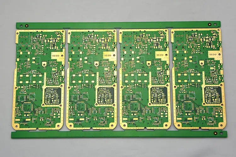
HDI board (High Density Interconnector), namely high-density interconnection board, is a circuit board with high circuit distribution density using micro blind hole embedding technology. The HDI board has an inner layer circuit and an outer layer circuit, and then uses drilling, hole metallization and other processes to connect the internal circuits of each layer.
HDI boards are generally manufactured by lamination method. The more times of lamination, the higher the technical level of boards. Ordinary HDI boards are basically stacked once, while high-order HDI boards are stacked twice or more, and advanced PCB technologies such as hole stacking, electroplating and hole filling, and laser direct drilling are also used. When the density of PCB is increased to more than eight layers, the cost of HDI manufacturing will be lower than that of traditional complex pressing process.
HDI board has higher electrical performance and signal correctness than traditional PCB. In addition, HDI board has better improvement for radio frequency interference, electromagnetic wave interference, electrostatic discharge, heat conduction, etc. High density integration (HDI) technology can make the terminal product design smaller, while meeting higher standards of electronic performance and efficiency.
HDI boards are plated with blind holes for secondary pressing, including first, second, third, fourth and fifth steps. The first level is relatively simple, and the process and process are easy to control. The main problems of the second order are: first, alignment, and second, punching and copper plating. There are many kinds of second order designs. One is stagger position of each order. When it is necessary to connect the next adjacent layer, it is connected in the middle layer through wires, which is equivalent to two first order HDIs. The second is that the two first order holes overlap, and the second order is realized by overlapping. The processing is similar to the two first order holes, but there are many process points to be specially controlled, that is, the above mentioned. The third method is to directly drill from the outer layer to the third layer (or N-2 layer). The process is different from the previous one, and the drilling is more difficult. For the third order, the second order analogy is.
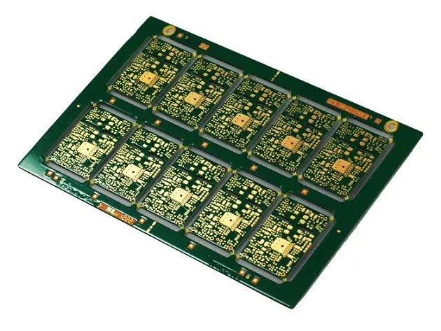
PCB, also known as printed circuit board (PCB) in Chinese, is an important electronic component, a support for electronic components, and a carrier for electrical connection of electronic components. The common PCB board is mainly FR-4, which is made of epoxy resin and electronic grade glass cloth.
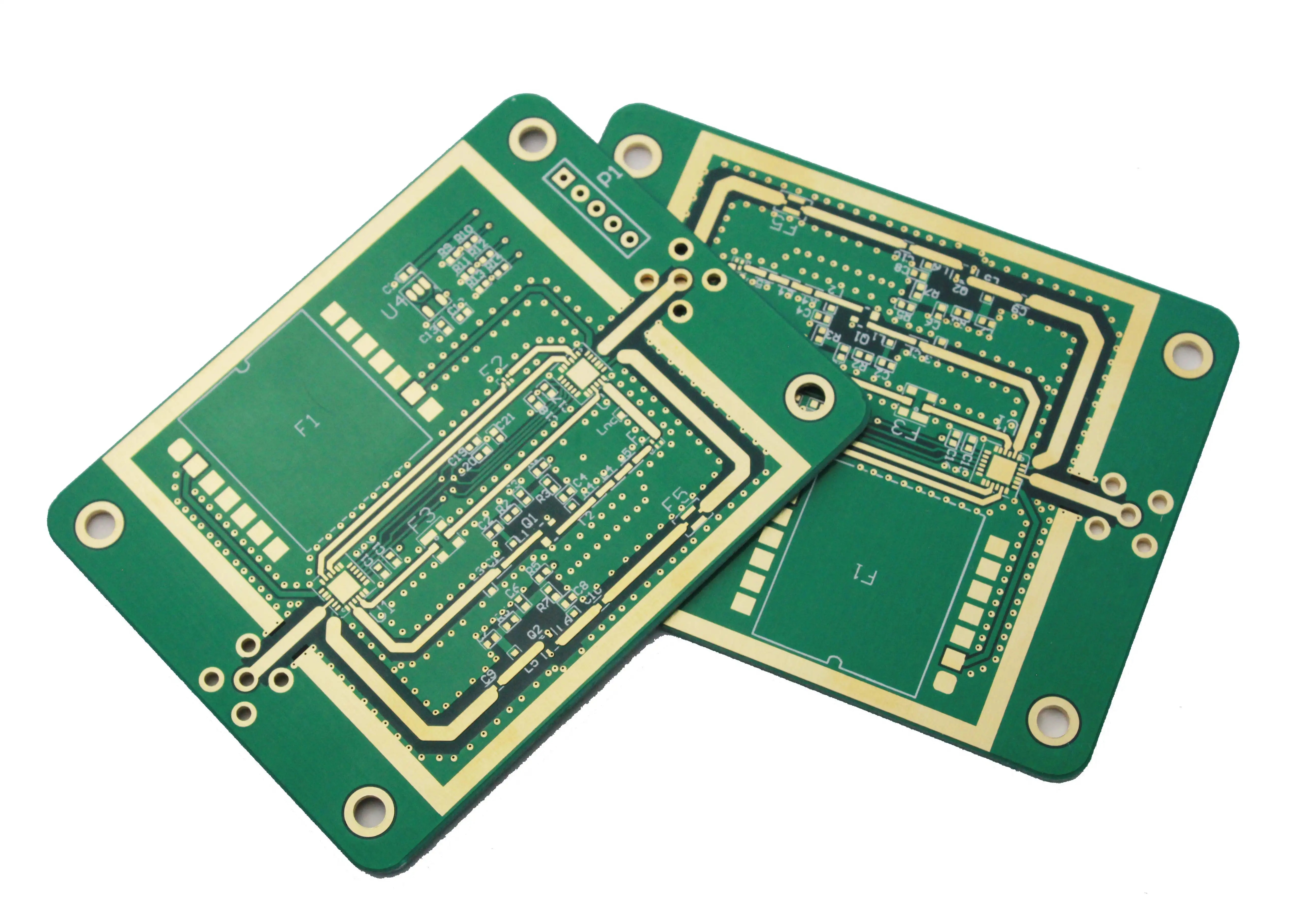
Pad is the most important basic unit in PCB design
According to different components and welding processes, pads in PCB can be divided into non via pads and via pads. Non via pads are mainly used for welding surface mounted components, and via pads are mainly used for welding pin type components. The selection of pad shape is related to the shape, size, layout, heating condition, force direction and other factors of components, and the designer needs to make the selection based on comprehensive consideration.
In most PCB design tools, the system can provide different types of pads for designers, such as round pads, rectangular pads, and octagonal pads.
1. Round pad
In printed circuit board, round pad is the most commonly used pad. For via pads, the main dimensions of round pads are via size and pad size. There is a proportional relationship between pad size and via size. For example, pad size is generally twice the space size. Non through-hole round pad is mainly used for test pad, locating pad and reference pad, and its main size is pad size.
2. Rectangular pad
Rectangular pads include square pads and rectangular pads. The square pad is mainly used to identify the first pin on the printed circuit board for installing components. The rectangular pad is mainly used as the pin pad of surface mount components. The size of the bonding pad is related to the pin size of the corresponding component, and the bonding pad size of different components is different. In order to avoid the phenomenon of offset and monument after over reflow soldering of devices, the pads at both ends of 0805 and below chip components with over reflow soldering should ensure thermal symmetry, and the width of the connection between the pad and the printed wire should not be greater than 0.3mm (for asymmetric pads).
3. Octagonal pad
Octagonal pad is seldom used in PCB. It is mainly set to meet the requirements of PCB wiring and bonding performance. In the PCB design process, designers can also use some special shaped pads according to the specific requirements of the design. For example, some pads with large heat output, large force and large current can be designed as teardrops.
PCB manufacturers, PCB designers and PCBA manufacturers will explain the differences between HDI boards and ordinary PCBs, as well as the role of pads.


Just upload Gerber files, BOM files and design files, and the KINGFORD team will provide a complete quotation within 24h.