
Professional PCB manufacturing and assembly
Building 6, Zone 3, Yuekang Road,Bao'an District, Shenzhen, China
+86-13410863085Mon.-Sat.08:00-20:00

Preventive Measures for Warpage of PCB and Classification of PCB Cladding
PCB manufacturers, PCB designers and PCBA processors will explain the preventive measures against warpage of PCB and the classification of PCB clad boards
The cause of PCB warping is, on the one hand, that the substrate used may be warped, and on the other hand, that warping is caused by thermal stress, chemical factors and improper process during processing. So, what are the precautions for PCB warping?
1. Prevent baseplate warping due to improper storage mode.
(1) During the storage of the CCL, if the storage environment humidity is high, the CCL will increase warpage due to moisture absorption. Therefore, for the copper clad laminate without moisture-proof packaging, it is necessary to pay attention to the warehouse conditions, minimize the warehouse humidity and avoid the bare placement of the copper clad laminate.
(2) Improper placement of CCL will increase warpage. If the copper clad plate is placed vertically or pressed with heavy objects, the warping deformation will be increased.
Solution: improve the storage environment, eliminate vertical placing and avoid heavy pressure.
2. Avoid warping caused by improper circuit design or processing technology.
For example, the conductive circuit diagram of the circuit board is unbalanced or the circuits on both sides are obviously asymmetric, which forms a large stress and causes warping; Warpage caused by higher processing temperature or greater thermal shock during the manufacturing process.
Solution: For circuit boards with large area of copper sheet in circuit graphics, it is better to grid the copper foil to reduce stress.
3. Eliminate substrate stress and reduce plate warpage during processing.
During the processing, the substrate is subject to the action of heat and various chemicals for many times. For example, if the substrate is heated due to water washing and drying after etching, and the hot air tin spraying is subject to large thermal impact, these processes may cause warping of the plate.
Solution: Since stress is the main cause of substrate warping, if the plate is baked before the CCL is put into use, the role of the baking plate is to fully relax the stress of the substrate, which is conducive to reducing the warping deformation of the substrate in the manufacturing process.
4. When wave soldering or dip soldering, the soldering temperature is too high and the operation time is too long, which will also increase the warpage of the substrate.
Solution: improve the wave soldering process, which requires the cooperation of the electronic assembly plant.
What are the classifications of PCB laminates?
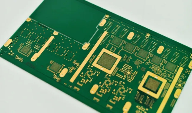
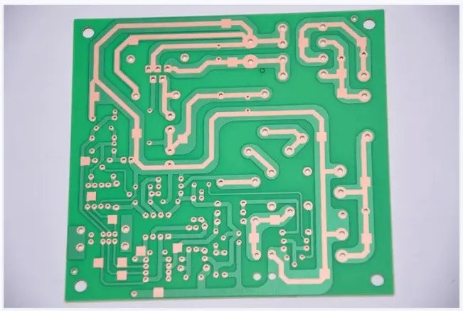
Copper clad laminate (CCL) is the most important and most used basic plate for PCB proofing; It is composed of copper foil, reinforcement material and adhesive. Its role is to support various components and realize electrical connection or electrical insulation between them. So, what are the classifications of PCB foil?
1. Classification by reinforcement
The most commonly used reinforcing materials for foil clad boards are alkali free, glass fiber products or paper. Therefore, the laminates can be divided into glass cloth based and paper based.
2. Classification by adhesive type
The adhesives used for the laminates mainly include phenolic, epoxy, polyester, polyimide, polytetrafluoroethylene resin, etc. Therefore, the laminates are also divided into phenolic, epoxy, polyester, polyimide, and polytetrafluoroethylene laminates.
3. Classification according to characteristics and uses of base materials
According to the burning degree of the substrate in the flame and after leaving the ignition source, it can be divided into general type and self extinguishing type; According to the bending degree of the substrate, it can be divided into rigid and flexible laminates; According to the working temperature and working environment conditions of the substrate, it can be divided into heat resistant, radiation resistant, high-frequency foil clad plates, etc. In addition, there are also laminates used in special occasions, such as prefabricated inner laminates, metal based laminates, and copper foil, nickel foil, silver foil, aluminum foil, copper foil, beryllium copper foil laminates.
4. Common foil clad plate model
According to GB4721-1984, the foil clad plate is generally represented by five English letters: the first letter C represents the copper foil covered, and the second and third letters represent the adhesive resin selected for the base material. For example, PE represents phenolic; EP is epoxy; UP represents unsaturated polyester; SI stands for organic silicon; TF stands for polytetrafluoroethylene, etc. The fourth and fifth letters indicate the reinforcement material selected for the base material. For example, CP stands for cellulose fiber paper; GC means alkali free glass fiber cloth, etc.
The two digits on the right of the horizontal line in the model indicate the product number of the same type but with different performance. For example, the number of copper clad phenolic paper laminate is O1~20, and the number of copper clad epoxy paper laminate is 21~30.
If the letter F is added after the product number, it indicates that the laminate is self extinguishing.
PCB manufacturers, PCB designers and PCBA processors will explain the preventive measures against warpage of PCB and the classification of PCB clad boards.


Just upload Gerber files, BOM files and design files, and the KINGFORD team will provide a complete quotation within 24h.