
Professional PCB manufacturing and assembly
Building 6, Zone 3, Yuekang Road,Bao'an District, Shenzhen, China
+86-13410863085Mon.-Sat.08:00-20:00

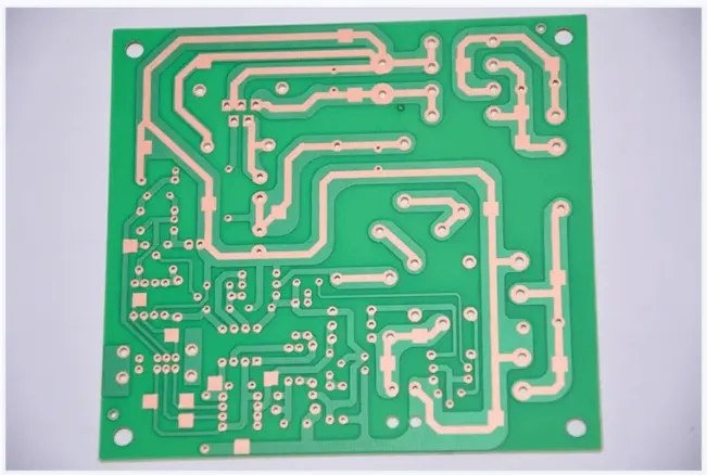
PCB noise reduction, electromagnetic and special device layout and welding defects
Nowadays, the sensitivity of electronic equipment is getting higher and higher, which requires the anti-interference ability of equipment to be stronger and stronger. Therefore, in PCB design, how to improve the anti-interference ability of PCB has become the focus of many engineers. The following are the methods summarized by PCB engineers to reduce noise and electromagnetic interference in PCB design:
1. If you can use low-speed chips, don't use high-speed chips.
2. The speed of control circuit can be reduced by stringing a resistor.
3. Use the clock with the lowest frequency meeting the system requirements.
4. The clock generator shall be as close as possible to the device using the clock.
5. Circle the clock area with a ground wire and keep the clock wire as short as possible.
6. The printed circuit board shall try to use 45 degree fold line instead of 90 fold line to reduce the external transmission and coupling of high-frequency signals.
7. The printed circuit board shall be partitioned according to the frequency and current switching characteristics, and the noise components shall be separated from the non noise components.
8. The clock, bus and chip selection signals shall be far away from I/O lines and connectors.
9. Analog voltage input line and reference voltage terminal shall be far away from digital circuit signal line.
10. The component pin shall be as short as possible, and the decoupling capacitor pin shall be as short as possible.
11. The key lines should be as thick as possible, and protective areas should be added on both sides. High speed lines should be short and straight.
12. The lines sensitive to noise shall not be parallel to the high current and high speed switching lines.
13. Do not run wires under quartz crystal or noise sensitive devices.
14. Do not form current loop around weak signal circuit and low-frequency circuit.
15. The signal shall not form a loop. If it is unavoidable, the loop area shall be as small as possible.
The above is what PCB engineers have summarized. Have you mastered some methods to reduce noise and electromagnetic interference in PCB design?
What are the layout requirements for special components of PCB?
Many special components are often used in PCB layout. Once the layout is not handled well, it will directly affect the performance and quality of PCB. What are the layout requirements for special components of PCB?
1. Layout requirements for crimping devices
(1) There shall be no components higher than 3mm around the crimping component surface, and no welding components around 1.5mm; There shall be no components within 2.5mm from the reverse side of the crimping device to the center of the pin hole of the crimping device.
(2) There shall be no components 1mm around crimping components.
2. Layout requirements of thermal sensors
(1) Thermal sensitive devices (such as electrolytic capacitors, crystal oscillators, etc.) shall be kept away from high thermal devices as far as possible.
(2) The thermal sensor shall be close to the element under test and away from the high temperature area to avoid the influence of other thermal power equivalent elements.
(3) Place the heating and heat-resistant devices close to the air outlet or on the top, and try to stagger them from other heating devices and thermal sensors in the air rising direction.
3. Layout requirements for devices with polarity
(1) The THD devices with polarity or directivity are aligned in the same direction in the layout.
(2) The direction of polar SMC on the board shall be as consistent as possible; Devices of the same type shall be arranged orderly and beautifully.
4. Layout requirements for through-hole reflow devices
(1) For PCB with non transfer edge size greater than 300mm, heavier components shall not be arranged in the middle of PCB as far as possible.
(2) To facilitate the insertion, the devices are arranged near the operation side of the insertion.
(3) The length direction of the device with longer size is consistent with the transmission direction.
(4) The distance between the pad edge of through-hole reflow soldering device and other SMT devices is>2mm.
(5) The distance between through-hole reflow devices is>10mm.
(6) The distance between the pad edge and the transfer edge of through-hole reflow devices is ≥ 10mm; The distance from the non transmitting side is ≥ 5mm.
The above are the layout requirements for special components of PCB, and I hope to help you.
What are the common welding defects of PCB?
Welding is an important process in PCB proofing. When we make PCB, we often see many welding defects. What are the common welding defects of PCB?
1. False soldering: There is an obvious black boundary between soldering tin and component lead or copper foil, and soldering tin is sunken towards the boundary.
Hazard: The circuit board does not work properly.
Reasons: 1) The component leads are not clean, tin plated or oxidized; 2) The printed board is not cleaned well, and the quality of the sprayed flux is poor.
2. Solder accumulation: the solder joint is loose, white and lusterless.
Hazard: insufficient mechanical strength, and possible faulty welding.
Reasons: 1) Poor solder quality; 2) Insufficient welding temperature; 3) The component leads are loose.
3. Too much solder: the solder surface is convex.
Hazard: Solder is wasted and may contain defects.
Cause: Solder removal was too late.
4. Too little solder: the welding area is less than 80% of the pad, and the solder does not form a smooth transition surface.
Hazard: The mechanical strength of the circuit board is insufficient.
Reasons: 1) Poor solder fluidity or premature solder withdrawal; 2) Insufficient flux; 3) Welding time is too short.
5. Rosin welding: the welding seam contains rosin slag.
Hazard: insufficient strength, poor continuity, and possible on-off.
Reasons: 1) Too many or invalid welding machines; 2) Insufficient welding time and heating; 3) The surface oxide film is not removed.
6. Overheating: white solder joints, no metallic luster, and rough surface.
Hazard: The pad is easy to peel off and its strength is reduced.
Cause: The power of the soldering iron is too high and the heating time is too long.
7. Cold welding: the surface is like bean curd slag particles, sometimes there may be cracks.
Hazard: low strength and poor conductivity.
Cause: The solder shakes before solidification.
8. Poor wetting: the interface between solder and weldment is too large and not smooth.
Hazard: low strength, no connection or on/off.
Reasons: 1) The weldment is not cleaned up; 2) Insufficient flux or poor quality; 3) The weldment is not sufficiently heated.
The above is the analysis of common welding defects of PCB. I hope you have some understanding of these defects and try to avoid them in practice.
PCB manufacturers, PCB designers and PCBA manufacturers explain PCB noise reduction, electromagnetic and special device layout and welding defects.


Just upload Gerber files, BOM files and design files, and the KINGFORD team will provide a complete quotation within 24h.