
Professional PCB manufacturing and assembly
Building 6, Zone 3, Yuekang Road,Bao'an District, Shenzhen, China
+86-13410863085Mon.-Sat.08:00-20:00

The Method of Successful PCB Design and Limit Temperature Test
PCB manufacturers, PCB designers and PCBA manufacturers will explain the successful methods of PCB design and limit temperature test
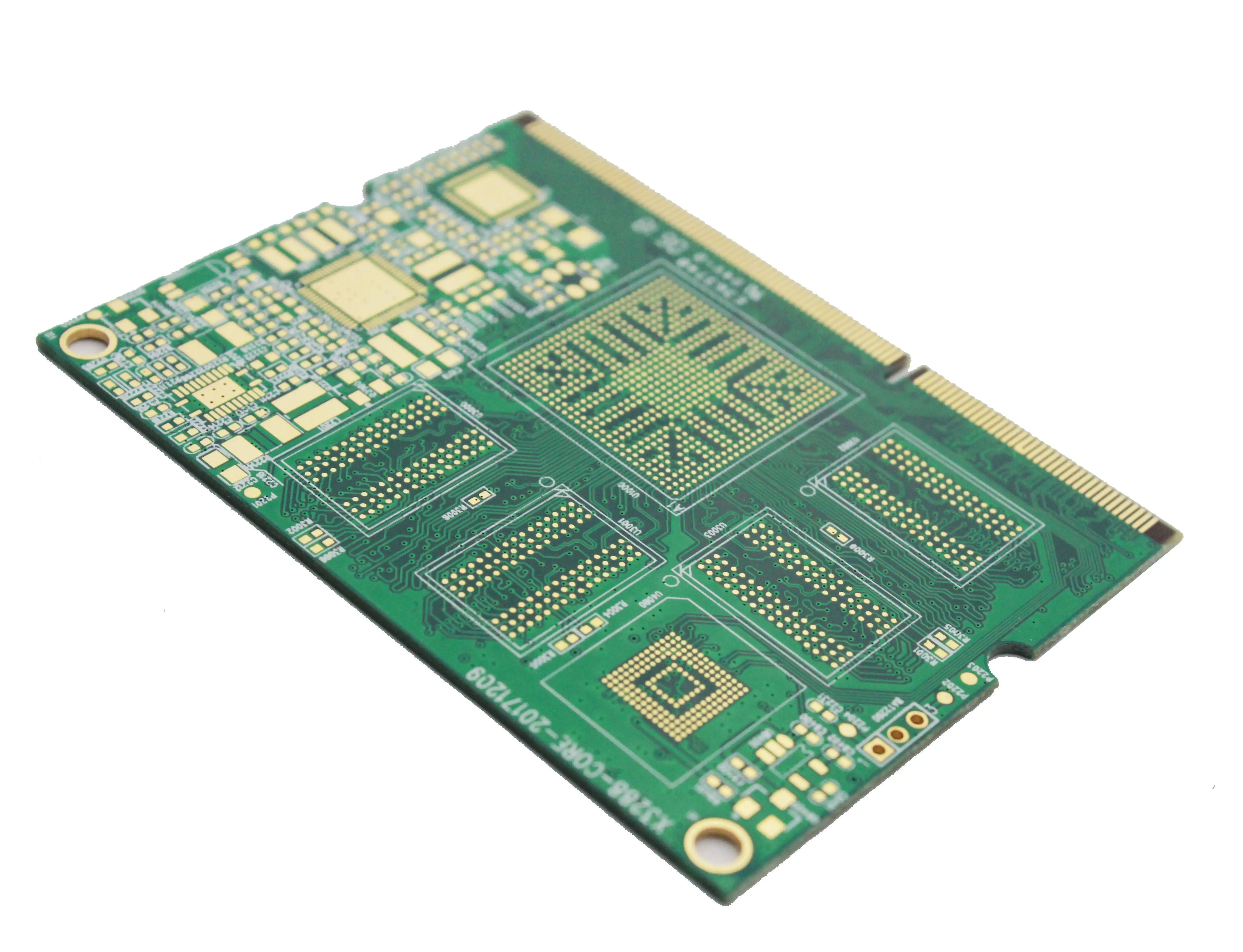
PCB design is an important step before PCB production. Once it is not well controlled, it will affect the subsequent production, and then affect the quality and performance of products. So, what are the methods for successful PCB design?
Method 1: Pay attention to the research of manufacturing method and chemical treatment process of the manufacturer
There are many engineers who really do not know the steps and chemical processing involved in generating PCB from their design files, resulting in inexperienced designers making needlessly complex design choices.
Method 2: Refer to the complete schematic diagram
Schematic diagram is a visual description of circuit, which can exchange information at many levels. When designing PCB layout, having a schematic diagram as a gold reference can make the work easier; Complete the connection with symbols; You don't have to think about connectivity at the same time when dealing with routing challenges.
Method 3: Use but do not completely rely on the automatic router
Most professional PCB CAD tools have automatic routing devices. In order to give full play to their role, the router parameters should be carefully and thoughtfully set for each task, and even each module in the single PCB design should be set separately. There is no basic general default setting suitable for any occasion.
Method 4: Geometric dimensions and current of circuit board
Most people who are engaged in electronic design know that, just like the river along the river, electronics may encounter choke points and bottlenecks. PCB designers occasionally produce similar electrical choke points in their PCB design. For example: 90 degree corner can be used where two fast 45s angles can be formed; The bending degree is greater than 90 degrees, forming a zigzag shape.
Method 5: Solve the fragmentation problem
Fragments are a manufacturing problem that can be best managed with the correct board design. When designing PCB layout, it is best to avoid leaving very narrow copper area. This area is usually caused by copper coating at the intersection of wire and pad gap. Set the minimum width of the copper sheet to exceed the minimum value allowed by the manufacturer, and your design should have no such problem.
Tip 6: Focus on DRC
Most design teams will eventually establish a set of design rules aimed at: standardizing the construction cost of bare boards and maximizing the yield; Assemble, inspect and test as consistently as possible.
Tip 7: Know the OEM factory you are using
A good OEM factory will provide some useful help and suggestions before you place an order, including how to improve your design to reduce design iterations, reduce problems encountered in the final debugging on the test bench, and improve the yield of the circuit board.
These are the successful methods of PCB design explained by senior engineers. I hope they can help you.
How to test the limit temperature of PCB?
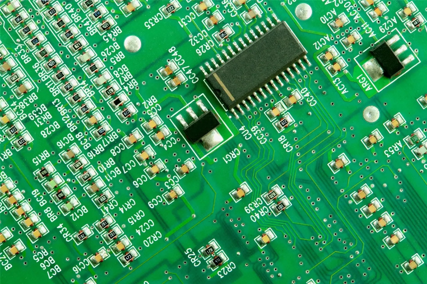
During the manufacturing process of PCB circuit board, because the PCB assembly board printed with solder paste and not soldered cannot fix the test end of the thermocouple, it is necessary to use the actual soldered product for temperature test. Then, how to test the limit temperature of PCB?
1、 Select test points: according to the complexity of the PCB assembly board and the number of channels of the collector, select at least three representative temperature test points that can reflect the high, medium and low temperatures on the PCB surface assembly board.
2、 Fixed thermocouple: weld the test ends of multiple thermocouples to the test points (solder joints) with high-temperature solder, and remove the solder on the original solder joints before welding; Or use high temperature adhesive tape to stick the test end of the thermocouple to each temperature test point on the PCB.
3、 Insert the other end of the thermocouple into 1, 2.3... of the machine table. The position of the jack or the socket of the collector shall be inserted, and the polarity shall not be reversed.
4、 Place the PCB assembly board of the tested surface on the conveyor chain/mesh belt at the inlet of the reflow welder, and then start the KIC temperature curve test program.
5、 With the PCB running, draw the real-time curve on the screen (when the device is equipped with KIC test software).
6、 When the PCB runs past the cooling area, pull the thermocouple wire to pull the PCB assembly board back. At this time, a test process is completed, and the complete temperature curve and peak temperature/schedule are displayed on the screen.
PCB manufacturers, PCB designers and PCBA manufacturers will explain the successful methods of PCB design and limit temperature test.


Just upload Gerber files, BOM files and design files, and the KINGFORD team will provide a complete quotation within 24h.