
Professional PCB manufacturing and assembly
Building 6, Zone 3, Yuekang Road,Bao'an District, Shenzhen, China
+86-13410863085Mon.-Sat.08:00-20:00

The number of PCB layers refers to the number of copper layers, and 6-layer pcb means that there are 6 copper circuit layers. It has a compact component layout and reduces manufacturing costs. Usually, electronic and cost-effective products use it. The 6-layer printed circuit board is the same as the 3-layer and 4-layer pcb. Both are multi-layer pcbs.
6-layer PCB board = standard 4-layer pcb + two additional signal layers. Therefore, a standard 1.6mm 6-layer PCB board stackup = top + bottom + 3 prepreg layers + 2 internal routing layers + 1 internal ground layer + 1 internal power layer + 2 core layers.
The benefits of 6-layer pcb stackup
6-layer pcb stackup can reduce space and make pcb more flexible. It also allows for more complex designs. Its various advantages are listed below.
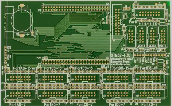
Component lead cutting machine pcb
A printed circuit board
Smaller size:
The 6-layer PCB is smaller and more flexible due to the paste of the PCB, which can achieve the same function. At the same time, 6-layer PCBs are manufactured with lightweight components, reducing the overall weight of these PCBs. Therefore, 6-layer pcb is ideal for many high-tech products.
More powerful:
This multilayer PCB has a very simple layout board. This facilitates higher transmission speeds for electronic devices.

Longer service life:
Multilayer PCB stacking protects the internal circuit boards from external influences. Multilayer PCBs use multiple layers of insulation between circuits. Protective materials and various adhesives are used to bond these layers. This reduces the wear and tear of the circuit board and prolongs its service life.
Reduce radiation:
Perfect PCB lamination design to minimize device radiation, especially in the lamination design of high frequency high speed circuit boards. In addition, if the impedance design is not reasonable, it is easy to cause more significant EMI radiation than standard PCB.
low cost:
A good multilayer PCB stack-up design can also reduce manufacturing costs by placing multiple circuits on the same board. And the 6-layer PCB stacking makes the connection process very simple on various machines. This simple design helps save space and materials that can be wasted when building large appliances.
Effectively reduce signal crosstalk:
Good PCB stack-up can mitigate impedance differences and signal crosstalk issues.
Factors that determine the design of a 6-layer pcb stackup

If done incorrectly or faulty, the 6-layer PCB laminate design procedure can lead to PCB fabrication failure. So there are a few things to consider as you go through the design process.
Design Configuration: This will help decide how to build the pcb stackup. You can choose from a variety of 6-layer pcb stackup combinations. The needs of your application dictate these settings.
Electrical Specifications: It is critical to consider how much current the 6-layer PCB will carry at any one time. This helps establish the correct signal path and routing for the draft.
Design and production costs: The cost of producing a 6-layer PCB stackup must be considered. If the design is more complex, the cost of creating the PCB stack will be higher.
Electrical Specifications: Since stacks are ideal for applications with varying temperature requirements, you must consider all aspects of thermal identification or specification when developing a 6-layer PCB stack.
Component Density: It is critical to consider the type and number of components mounted on the PCB stack-up, as this will facilitate electrical connections.
Application of 6-layer PCB
Defibrillator
A printed circuit board
As the demand for electronic equipment grows, so does the demand for multilayer circuit boards from many manufacturers. Here are some applications where you can use 6-layer PCB lamination.
Consumer electronic equipment: such as mobile phones, refrigerators, computers, ovens, etc.
Communication facilities: such as GPS, satellite, etc.
Medical equipment: such as X-ray machines, infrared lamps, etc.
Transportation: such as cars, planes, high-speed rail, etc.
What are the steps of 6-layer PCB design?
Editing Diagrams: Double-check the schematic when you're done creating it.
Create a new PCB file and create a 6-layer PCB layer structure as follows: After the creation, the schematic netlist can be imported into the PCB file for 6-layer PCB production.
Layout: In 6-layer PCB manufacturing, the first prerequisite for layout is good partitioning. Separating analog and digital equipment can also help prevent interference. Anti-jamming is especially necessary, since digital signals can cause significant interference.
Ground plane fabrication: There are two ground planes on a 6-layer PCB: AGND and DGND. The two are usually separate, on the second and fourth floors, respectively. Connection techniques are rarely used because the pads create capacitive effects and increase interference.
Making the power supply layer: Since the working voltage value of the multilayer PCB board is more than one, the power supply layer must be divided.
Routing: Make sure power and ground planes are good, and route important high-speed signal lines to internal signal layers.
Perform a DRC check: This step is critical for 6-layer PCB production. The PCB drawing must be verified after it is completed.
6 layer pcb prototype price
kingford is a famous Chinese 6-layer pcb manufacturer. We provide pcb prototyping at low cost, high quality and fast turnaround. PCB Assembly Prototypes enable you to quickly test your stacks and designs, find bugs and defects in real-time, and reduce losses before mass production.

Advantages of Copper PCBs
Jun 20,2022


Just upload Gerber files, BOM files and design files, and the KINGFORD team will provide a complete quotation within 24h.