
Professional PCB manufacturing and assembly
Building 6, Zone 3, Yuekang Road,Bao'an District, Shenzhen, China
+86-13410863085Mon.-Sat.08:00-20:00

How to repair the uneven coverage of PCB anti soldering paint found by PCB manufacturers?
PCB manufacturer, PCB designer and PCBA manufacturer explain how to repair the uneven coverage of PCB solder mask
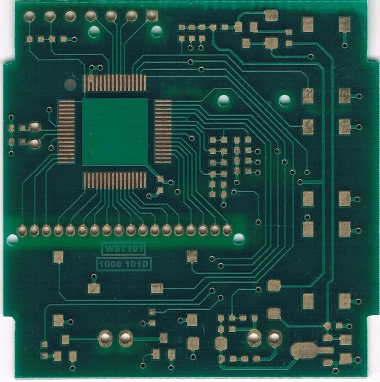
With regard to anti soldering paint, if PCB shipped from PCB board factory is found to have uneven coverage of anti soldering paint, how do you generally repair it? If green oil bubbles after wave soldering of PCB, can it be repaired generally? Is there any relevant specification that green paint repair is feasible? How to make up?
If there is no metal leakage on the circuit board, it should not be repaired. It's just that the appearance is not beautiful. The customer's acceptance is not a problem. If you really want to repair the damaged metal surface, you should first clean the exposed metal surface and prepare a stop welding paint mixed with hardener, and then repair it with a brush. After the repair is completed, send it to the oven to bake and harden. The above is a possible way to deal with holes, but there is no way to answer your question about uneven coverage. Unless otherwise specified, most circuit board products are accepted on the basis of no copper leakage. The solder mask paint will have a certain degree of thickness difference. If the quality is too poor, it must be scrapped. I'm afraid it cannot be repaired.
Theoretically, if the green paint peels off after wave soldering, the surface will be stained with solder. After cleaning, it should be repaired moderately. It should be functional, but whether the customer can accept this quality situation must be communicated. At present, there is no clear public specification for such repair work, and both parties must jointly establish an acceptable standard. I haven't heard about a special repair pen. Generally, people use the brush repair method, but it is recommended that the pen should be strong and not lose its hair. Generally, the brush used for repair will be reused, so it must be cleaned after use to avoid residue, or subsequent repair will cause pollution problems.
If there is a large number of fixed area repair or missing printing needs, it is recommended to make repair screen for printing repair, which is not only neat but also stable. As for products that cannot be printed after assembly, brush repair is still a feasible way at present. The above is for your reference.
The PCB manufacturer, PCB designer and PCBA manufacturer explain how to repair the uneven coverage of PCB solder mask.


Just upload Gerber files, BOM files and design files, and the KINGFORD team will provide a complete quotation within 24h.