
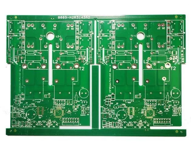
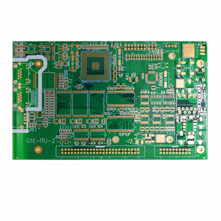
Professional PCB manufacturing and assembly
Building 6, Zone 3, Yuekang Road,Bao'an District, Shenzhen, China
+86-13410863085Mon.-Sat.08:00-20:00

Five Common Applications of PCB Surface Treatment Process
The surface treatment process will affect the production, assembly and final use of PCB. The following details the application occasions of five common surface treatment processes.
1. Hot air leveling; Hot air leveling once played a leading role in PCB surface treatment process. In the 1980s, more than three quarters of PCBs used the hot air leveling process, but the industry has been reducing the use of the hot air leveling process over the past decade. It is estimated that 25% - 40% of PCBs currently use the hot air leveling process. The hot air leveling process is dirty, smelly and dangerous, so it has never been a favorite process, but it is an excellent process for larger components and wires with large spacing. In PCB with high density, the flatness of hot air leveling will affect the subsequent assembly; Therefore, HDI boards generally do not use hot air leveling process. With the progress of technology, the hot air leveling process for QFP and BGA with smaller assembly spacing has emerged in the industry, but it is rarely used in practice. At present, some factories use organic coating and electroless nickel plating/gold leaching process to replace the hot air leveling process; Technological development has also led some factories to adopt tin dipping and silver dipping processes. With the trend of lead-free in recent years, the use of hot air leveling is further restricted. Although the so-called lead-free hot air leveling has occurred, it may involve the compatibility of the equipment.
2. Organic coating; It is estimated that about 25% - 30% of PCBs currently use organic coating technology, and the proportion has been rising (it is likely that organic coating has now surpassed hot air leveling and ranked first). The organic coating process can be used on low technology PCB or high technology PCB, such as single side TV PCB and high-density chip packaging board. For BGA, organic coating is also widely used. If PCB has no functional requirements for surface connection or storage period limitation, organic coating will be the most ideal surface treatment process.
3. Electroless nickel plating/gold immersion; The electroless nickel/gold plating process is different from the organic coating process. It is mainly used on boards with connection functional requirements on the surface and a long storage period, such as the mobile phone key area, the edge connection area of the router shell and the electrical contact area of the elastic connection of the chip processor. Due to the flatness of hot air leveling and the removal of organic coating flux, electroless nickel/gold plating was widely used in the 1990s; Later, due to the emergence of black disk and brittle nickel phosphorus alloy, the application of electroless nickel plating/gold leaching process has decreased. However, almost every high-tech PCB factory has electroless nickel plating/gold leaching line. Considering that solder joints will become brittle when copper tin intermetallics are removed, there will be many problems at relatively brittle nickel tin intermetallics. Therefore, portable electronic products (such as mobile phones) almost all adopt copper tin intermetallic compound solder joints formed by organic coating, silver dipping or tin dipping, while the key area, contact area and EMI shielding area are formed by electroless nickel/gold dipping. It is estimated that about 10% - 20% of PCBs currently use the electroless nickel/gold plating process.
4. Silver immersion; Silver dip is cheaper than electroless nickel/gold dip. If PCB has functional requirements for connection and needs to reduce costs, silver dip is a good choice; In addition, silver immersion has good flatness and contact, so silver immersion process should be selected. There are many silver dipping applications in communication products, automobiles, and computer peripherals, as well as in high-speed signal design. Silver immersion can also be used in high frequency signals because of its excellent electrical properties that other surface treatments cannot match. EMS recommends the silver immersion process because it is easy to assemble and has good inspectability. However, due to the defects of silver immersion, such as tarnish and solder hole, its growth is slow (but not decreased). It is estimated that about 10% - 15% of PCB currently use silver immersion process.
5. Tin dipping; It has been nearly ten years since tin was introduced into the surface treatment process. The appearance of this process is the result of the requirements of production automation. Tin dipping does not bring any new elements into the welding area, which is especially suitable for communication backplane. Tin will lose solderability beyond the storage period of the board, so better storage conditions are required for tin dipping. In addition, the use of tin dipping process is restricted due to the presence of carcinogens. It is estimated that about 5% - 10% of PCB currently use tin dipping process. V Conclusion With the increasing customer requirements, stricter environmental requirements and more and more surface treatment processes, the choice of a promising and more versatile surface treatment process seems a bit confusing at present. It is also impossible to accurately predict where the PCB surface treatment process will go in the future. In any case, meeting customer requirements and protecting the environment must be done first!
PCB manufacturing, PCB design and PCBA processing manufacturers explain five common use occasions of PCB surface treatment process.
How to learn PCB layout
Nov 08,2022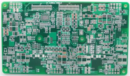


Just upload Gerber files, BOM files and design files, and the KINGFORD team will provide a complete quotation within 24h.