
Professional PCB manufacturing and assembly
Building 6, Zone 3, Yuekang Road,Bao'an District, Shenzhen, China
+86-13410863085Mon.-Sat.08:00-20:00

6 Steps of Basic Manufacturing Process of Layered PCB
Generally, the fabrication method of multilayer board is to make the inner layer pattern first, then make a single or double sided substrate by printing and etching, and incorporate it into the designated interlayer, and then heat, pressurize and glue it. As for the later drilling, it is the same as the plating through hole method of double-sided board. 1. First, the FR4 circuit board of the base layer must be manufactured. After the plating of perforated copper in the base layer is completed, the holes are filled with resin, and the surface lines are formed by subtractive etching. In this step, except that the perforation is filled with resin, other steps are the same as those of common FR4 circuit boards. 2. Apply photosensitive epoxy resin as the first layer of insulation FV1. then
Generally, the fabrication method of multilayer board is to make the inner layer pattern first, then make a single or double sided substrate by printing and etching, and incorporate it into the designated interlayer, and then heat, pressurize and glue it. As for the later drilling, it is the same as the plating through hole method of double-sided board.
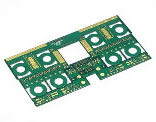
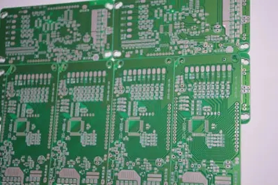
Multilayer circuit board
First, the FR4 circuit board of the base layer must be manufactured. After the plating of perforated copper in the base layer is completed, the holes are filled with resin, and the surface lines are formed by subtractive etching. In this step, except that the perforation is filled with resin, other steps are the same as those of common FR4 circuit boards.
2. Apply photosensitive epoxy resin as the first layer of insulation FV1. After drying, the mask is used for exposure. After exposure, the solvent is used for developing to form the lower hole of the bolt hole. The resin shall be hardened after opening.
3. The epoxy resin surface is roughened by permanganate etching. After etching, a layer of copper is formed on the surface with electroless copper for subsequent copper electroplating steps. After the copper conductor layer is formed by electroplating, the conductor is formed by subtractive etching method as the base layer.
4. The second insulating layer is coated, and the lower hole of the bolt hole is formed by using the same exposure development step.
5. If a hole is needed, the hole can be formed by drilling, and then the wire can be formed by electroplating copper etching.
6. Apply tin proof paint on the outermost layer of the circuit board, and expose the contact part by exposure development.
If the number of layers increases, the above steps are basically repeated. If there are layers on both sides, the insulating layer must be coated on both sides of the base layer, but the electroplating process on both sides can be carried out at the same time.
Circuit board manufacturing, circuit board design and PCBA processing manufacturers will explain the six major steps of the basic manufacturing process of layer added circuit boards.


Just upload Gerber files, BOM files and design files, and the KINGFORD team will provide a complete quotation within 24h.