
Professional PCB manufacturing and assembly
Building 6, Zone 3, Yuekang Road,Bao'an District, Shenzhen, China
+86-13410863085Mon.-Sat.08:00-20:00

Explain in detail the causes of PCB bursting and its solutions
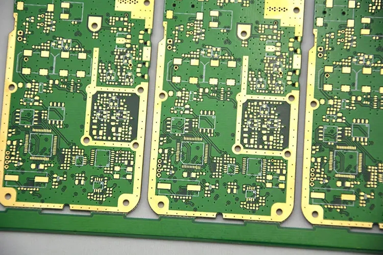
The Cause of PCB Burst and Its Solution
The main reason why PCB board will pop or delaminate is that ① the board absorbs water ② α 2/z-CTE is too large, and 70% of the defects are caused by "board water absorption". Other reasons, such as uneven expansion and contraction of PCB structure, uneven heat and cold, process injury and poor blackening, can not be ruled out, but the ratio is not too high.
Why is "water" the main cause of PCB bursting?
When "water" is below 100 ° C, it has little effect on the bursting of plates. When the temperature exceeds 100 ° C, "water" will become the plasticizer of the resin. When the resin absorbs more water, Tg will drop (△ Tg should be less than 5 ° C) and the rubber state will arrive early, which will lead to the instant swelling in the Z direction of the plate and rapid cracking (most likely between 100 ° C and Tg). When the water vapor exceeds 100 ° C, the air pressure (psi) will increase in equal proportion.
Generally, CTE (coefficient of expansion) of X and Y of the plate is relatively stable, about 15~16ppm/° C. In addition, the hidden water in the plate will also become the plasticizer of the resin, helping Zhou to be evil together with the external water.
When the resin temperature exceeds Tg point, it will change into rubber gel state. At this time, the "water" split plate has changed into a supporting role, and most of the water at this time has also changed into steam to evaporate. Besides, the rubber gel state is soft, and it is not easy to have a split plate.
Where does PCB "water" come from?
Since "water" is so important for bursting boards, we should carefully study where the water comes from. As far as we generally know, most of the "water" may come from the outside world, which may be inhaled and attached during PCB manufacturing, or diffused into the environment during PCB storage; However, the internal structure of the board is easy to store water, which is also one of the possible reasons; Another thing you may not think of is that the molecular formula of PCB resin also contains water molecules, which will generate water by itself after heating. Therefore, it is concluded that the "water" absorption and water storage of the board are:
1. The structural water of the resin molecule itself (water molecules have been hidden in the far polar part of the resin molecular structure, so long as OH is contained in the chemical formula, it is possible to form water).
2. The joint of resin and glass fiber is easy to store water (the plate is woven with a strip of resin and a strip of glass fiber by warp and weft. If the weaving is not dense enough, there will be gaps. It is generally recommended to use flat fiber cloth with low air permeability to store water.).
3. The interface between resin and copper foil is also easy to trap water.
4. There will be water in the cavity of the plate.
Improvement Plan for PCB Water absorbing Explosion Board Baking
Since "water" is the main cause of PCB bursting, so as long as the moisture in the PCB is removed, most of the bursting problems can be solved, and [baking] is the best way to remove the moisture outside the PCB. Since the purpose of baking is to remove moisture, the baking conditions should meet the following requirements:
1. The baking temperature is heated to a little more than 100 ° C (105 ° C is recommended, because the temperature of the oven may have errors), so that the water can be turned into steam and can be easily dissipated.
2. When baking, it is better to put each plate separately, so that the water can evaporate easily. If PCBs overlap, water will not escape effectively.
3. The oven must be equipped with an exhaust device, otherwise it will be useless if the oven is full of steam during baking.
Control the water absorption conditions from the selection and manufacturing process of PCB boards
Although baking is the best way to improve the bursting of PCB, baking not only wastes time, but also wastes equipment and manpower. It is also a problem that the Tg value will decrease after PCB baking. A better way is to control the water absorption conditions from the selection and manufacturing process of PCB boards.
1. If the plate itself has polarity, it is easy to absorb water. Try to select the resin that will not absorb water to prevent the board from absorbing water.
2. Open (flat) fiber cloth can be selected. Reduce the gap between resin and glass fiber interface to reduce the possibility of water storage.
3. PCB pressing process control. For multilayer boards whose PCB has completed pressing and post baking, the sample can be taken to measure the Tg value twice with the same method and machine; Where the △ Tg of Tg2-Tg1 exceeds 2~3 ° C (different according to different plates), it means that the curing reaction (Hardening including polymerization and cross-linking) in the pressing process is not in place, and such immature plates will easily absorb water and burst.
4. Measure the Tg value of the problem board according to the TMA method in Section 2.4.24.1 of the TM-650 Test Manual, and compare it with the specification value of the supplier. Where the measured value is lower than the specification value by more than 5 ° C, it means that the problem plate has a focus of water absorption. The water fractal in the resin is the same as the plasticizer, which will not only lower Tg, but also make the rubber state come earlier.
Multi layer PCBs stored for more than three months may exhibit stress concentration (from pressing) and the fact that water absorption (will increase Z-expansion). Explosion proof measures of pre welding baking (105 ° C+24 hours) shall be taken, or 50 mobile phone boards of the leveler shall be pressed and baked in nitrogen for 2 hours at 185 ° C+70PSI. For boards with the client more than three months old, baking before soldering will reduce the number of board bursts. Baking will not only increase the cost but also be detrimental to OSP. When baking, it is necessary to bake single pieces separately to facilitate the full discharge of water.


Just upload Gerber files, BOM files and design files, and the KINGFORD team will provide a complete quotation within 24h.