
Professional PCB manufacturing and assembly
Building 6, Zone 3, Yuekang Road,Bao'an District, Shenzhen, China
+86-13410863085Mon.-Sat.08:00-20:00

Solder paste process, technical requirements and scope of application
PCB manufacturers and PCB designers explain the solder paste process, technical requirements and scope of application
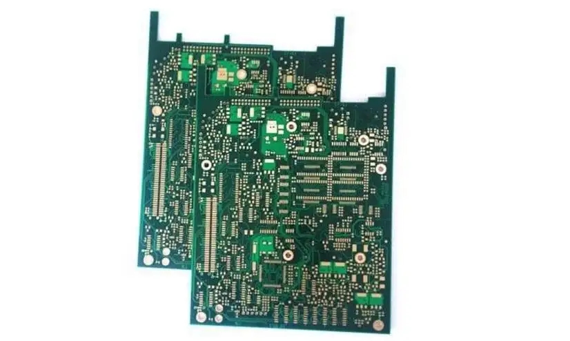
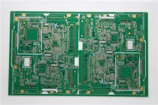
Solder paste process plays a very important role in the whole PCBA processing process, and plays a key role in the welding reliability of bonding pads and components.
1: Process Purpose
Apply an appropriate amount of Sn/Pb solder paste evenly on the PCB pad to ensure that the pad corresponding to the patch assembly and PCB has good electrical connection and sufficient mechanical strength.
2: Technical Requirements
1: The amount of solder paste applied is uniform and consistent. The pad graphics should be clear, and adjacent graphics should not be stuck. The solder paste pattern should be consistent with the pad pattern and should not be misaligned.
2: In general, the amount of solder paste per unit area on the pad should be about 0.8mg/mm2. For components with narrow spacing, it shall be about 0.5mg/mm2.
3: A certain deviation can be allowed between the solder paste printed on the substrate and the desired weight value. The area of each pad covered by the solder paste should be more than 75%. When using the cleaning free technology, it is required that all the solder paste should be on the pad.
4: After the solder paste is printed, there shall be no serious collapse, the edge shall be neat, and the dislocation shall not be greater than 0.2 ㎜. For the bonding pads of components with narrow spacing, the dislocation shall not be greater than 0.1 ㎜. The substrate surface shall not be contaminated by solder paste. When the cleaning free technology is adopted, the solder paste can be completely located on the bonding pad by reducing the opening size of the template.
3: Methods of applying solder paste and application scope of various methods
There are two methods to apply solder paste: drip coating (i.e. injection coating, which can be divided into manual and automatic drip coating machine) and metal template printing. The application scope of the two methods is as follows:
1: Manual drop coating method -- the development stage of model prototype and performance prototype for small batch production or new products, as well as repair and replacement of components during production.
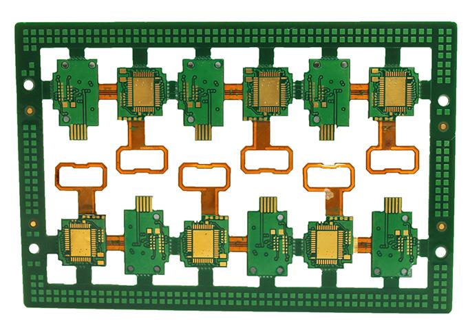
2: Metal template printing -- used for large and medium batch production, products with high assembly density, and products with multi lead narrow spacing devices (narrow spacing devices refer to surface mounted devices with a pin center distance of not more than 0.65mm; they also refer to length × Width not greater than 1.6 × 0.8mm surface assembled components). Since the quality of metal template printing is relatively good and the service life of metal template is long, the metal template printing process should be preferred.a


Just upload Gerber files, BOM files and design files, and the KINGFORD team will provide a complete quotation within 24h.