
Professional PCB manufacturing and assembly
Building 6, Zone 3, Yuekang Road,Bao'an District, Shenzhen, China
+86-13410863085Mon.-Sat.08:00-20:00

Radio frequency (RF) PCB design, with many uncertainties in the current published theory, is often described as a "black art". Generally, for circuits (including low-frequency and low-frequency digital circuits) in the frequency band below microwave, careful planning on the premise of fully mastering various design principles is the guarantee of successful design at one time. For PC type digital circuits with frequencies above microwave and high frequency, 2 to 3 versions of PCB are required to ensure circuit quality. For RF circuits in the frequency band above microwave, more versions are often required and constantly improved, and on the premise of considerable experience. This shows the difficulties in RF electrical design.
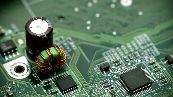
Typical RF board
RF design
Wireless Internet Access Module
PCB design
Before layout, it is necessary to be familiar with product architecture and signal flow
1 Common problems in RF circuit design
1.1 Interference between digital circuit module and analog circuit module
If the analog circuit (RF) and digital circuit work separately, they may work well respectively. However, once they are placed on the same circuit board and work together with the same power supply, the whole system is likely to be unstable. This is mainly because the digital signal frequently swings between the ground and the positive power supply (>3V), and the period is very short, usually nanosecond. Because of the large amplitude and short switching time, these digital signals contain a large number of high-frequency components independent of the switching frequency. In the analog part, the signal transmitted from the wireless tuning loop to the wireless device receiving part is generally less than 1 μ V。 Therefore, the difference between digital signal and RF signal will reach 120 dB. Obviously, if the digital signal cannot be separated from the RF signal well, the weak RF signal may be damaged. In this way, the working performance of the wireless device will deteriorate, or even cannot work at all.
Common interference phenomena
1.2 Noise interference of power supply
RF circuit is very sensitive to power supply noise, especially to burr voltage and other high-frequency harmonics. The microcontroller will suddenly absorb most of the current in a short time within each internal clock cycle, because modern microcontrollers are made with CMOS technology. Therefore, suppose a microcontroller operates at an internal clock frequency of 1 MHz, at which it will extract current from the power supply. If proper power decoupling is not adopted, voltage burr on the power line will be caused. If these voltage burrs reach the power supply pin of the RF part of the circuit, it may lead to work failure in serious cases.
Pay attention to the rules of RF chip power supply layout and capacitor layout
High speed clock important signal wiring runs on the inner layer with complete reference plane and package protection
1.3 Unreasonable ground wire
If the ground wire of RF circuit is handled improperly, some strange phenomena may occur. For digital circuit design, most digital circuits perform well even without ground layer. In the RF band, even a short ground wire can act as an inductor. Roughly calculated, the inductance per mm is about 1 nH, and the inductance of 10 mm PCB circuit is about 27 Ω at 433 MHz. If the ground layer is not used, most of the ground wires will be longer, and the circuit will not have the designed characteristics.
1.4 Radiated interference of antenna to other analog circuits
In PCB circuit design, there are usually other analog circuits on the board. For example, many circuits have analog to digital converters (ADC) or digital to analog converters (DAC). The high-frequency signal from the antenna of the RF transmitter may reach the analog input terminal of ADC. Because any circuit line may send or receive RF signals like an antenna. If the processing of ADC input terminal is unreasonable, RF signal may self excite in the ESD diode input by ADC, causing ADC deviation.
2 RF circuit design principle and scheme
2.1 RF Layout Concept
When designing RF layout, the following general principles must be satisfied first
(1) Isolate the high power RF amplifier (HPA) and low noise amplifier (LNA) as much as possible. In a word, keep the high power RF transmitting circuit away from the low power RF receiving circuit.
Design of PA Offset Quarter Wavelength in Power Amplifier
Straight line layout principle
Vertical arrangement of amplifier bias inductor
Wrong amplifier offset layout
(2) Make sure that the high power area on the PCB has at least one whole ground. It is better to have no via on it. Of course, the larger the copper foil area, the better.
Sufficient GND vias to improve signal grounding and heat dissipation
RF filter shall be fully grounded
(3) Decoupling circuits and power supplies is also extremely important.
(4) RF outputs usually need to be away from RF inputs.
(5) Sensitive analog signals should be as far away from high-speed digital signals and RF signals as possible.
2.2 Design principles of physical partition and electrical partition
Design zones can be decomposed into physical and electrical zones. Physical partition mainly involves component layout, direction and shielding; The electrical partition can be further divided into power distribution, RF wiring, sensitive circuits and signals, and grounding partitions.
2.2.1 Principle of physical partition
(1) Principle of component location layout. Component layout is the key to achieving an excellent RF design. The most effective technology is to first fix the components on the RF path and adjust their direction, so as to minimize the length of the RF path, keep the input away from the output, and separate the high power circuit and low power circuit as far as possible.
RX/TX digging or shielding isolation
(2) PCB stack design principles. The most effective circuit board stacking method is to arrange the main ground (main ground) on the second layer below the surface layer, and arrange RF lines on the surface layer as much as possible. Minimizing the size of vias on the RF path can not only reduce the path inductance, but also reduce the number of solder joints on the main ground, and reduce the chance of RF energy leakage to other areas in the laminate.
Common RF plate model
Rational Ro4350 RF stack and impedance linewidth design
(3) RF devices and their RF wiring layout principles. In physical space, linear circuits such as multistage amplifiers are usually sufficient to isolate RF regions from each other, but duplexers, mixers, and IF amplifiers/mixers always have multiple RF/IF signals interfering with each other, so care must be taken to minimize this impact. RF and IF traces should cross as much as possible and be separated by a piece of land as much as possible. Correct RF path is very important to the performance of the whole PCB, which is why component layout usually takes up most of the time in the design of cellular telephone PCB.
The design of one out of two circuit requires attention to open microstrip
2.2.2 Principles of electrical zoning
(1) Power transmission principle. The DC current of most circuits in cellular phones is relatively small, so the wiring width is usually not a problem. However, a large current line as wide as possible must be set separately for the power supply of the high power amplifier to minimize the transmission voltage drop. In order to avoid too much current loss, multiple through holes are required to transfer current from one layer to another.
(2) Power decoupling of high power devices. If it cannot be fully decoupled at the power supply pin of the high power amplifier, the high power noise will radiate to the whole board and cause various problems. The grounding of high power amplifier is very critical, and a metal shield is often required for it.
(3) RF input/output isolation principle. In most cases, it is also critical to ensure that the RF output is kept away from the RF input. This also applies to amplifiers, buffers, and filters. In the worst case, if the outputs of amplifiers and buffers are fed back to their inputs with appropriate phase and amplitude, they may generate self-excited oscillation. In the best case, they will be able to work stably under any temperature and voltage conditions. In practice, they may become unstable and add noise and intermodulation to the RF signal.
Input and output need to be separated
3 Conclusion
In a word, RF circuit is different from low-frequency circuit and DC circuit because of its distributed parameter circuit, skin effect and coupling effect. Therefore, these problems should be paid special attention to when designing the RF circuit PCB, so as to ensure the effectiveness and accuracy of the circuit design. E-Link network data transmitter can also be used to build a new generation of Ethernet measurement and control system, to transform the existing distributed control system composed of field bus and to develop production network measurement and control equipment. It will promote the intellectualization and networking of household appliances and make profound changes in people's lifestyle.
Our circuit provides one-stop proofing and small and medium-sized batch production and manufacturing services such as SMT chip proofing, PCBA processing, smt chip processing, electronic component purchasing, DIP post welding and assembly testing.

Width setting standard of PCB process edge
Nov 01,2022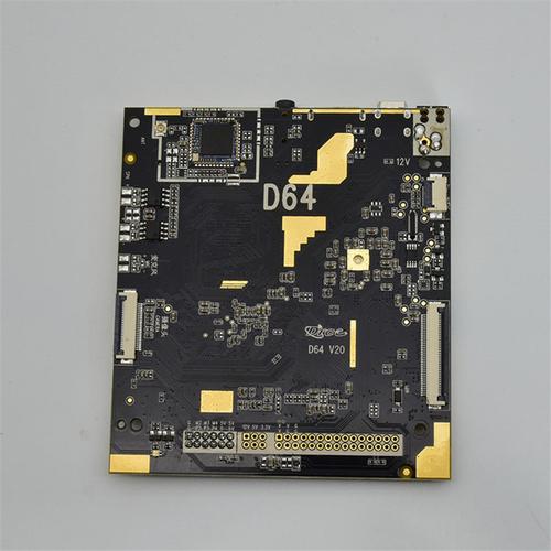


Just upload Gerber files, BOM files and design files, and the KINGFORD team will provide a complete quotation within 24h.