
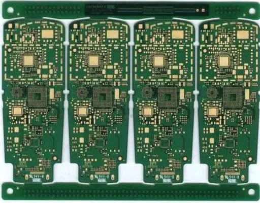
Professional PCB manufacturing and assembly
Building 6, Zone 3, Yuekang Road,Bao'an District, Shenzhen, China
+86-13410863085Mon.-Sat.08:00-20:00


Cause Analysis of PCBA Assembly Explosion
To understand the use of high CTI special printed boards, you must first understand CTI and its principle, copper clad laminate and PCB manufacturing process.
CTI and its principle
CTI refers to the relatively rapid leakage index or relative leakage tracking index. It refers to the highest voltage value of PCB substrate surface that withstands 50 drops of electrolyte without forming leakage hum. This value must be a multiple of 25 and is tested according to IEC-112 standard.
When the surface of the polymer solid insulating material base material of copper clad laminate is polluted by solution pollutants with positive and negative ions during the shelf life, the leakage current of the surface is much larger than that of the clean surface when a certain voltage is applied. According to the heat formula Q=R * I square, when the leakage current increases, the heat generated by the leakage current increases, and the speed of evaporation of wet pollutants accelerates, which is the uneven drying state of the polymer material surface, This may result in the formation of drying zones or spots on local surfaces. The dry area increases the surface resistance, so the electric field becomes uneven, and flashover discharge points are generated. Under the combined action of electric field and heat, the surface of insulator material is forced to talk, and the carbide resistance is small, which increases the electric field strength formed by the voltage applied tip, so flashover discharge points are more likely to occur. In such a vicious cycle, it is known that the surface resistance between the electrodes causing the applied voltage is damaged, forming a conductive channel and generating leakage marks.
Once the base material of the copper clad polymer solid insulating material has leakage marks, there are three kinds of deterioration phenomena. First, there are carbonized black dendritic conductive channels. After several times of continuous tapping, the conductive channels continue to grow. When the two poles are bridged, the material can be damaged by breakdown; However, under the action of multiple discharge points, the material is ignited and destroyed; Third, there are some pits in the material. When the placing continues, the pits deepen, causing electrical corrosion, and the advantages are damaged by clicking, sometimes without being broken down.
According to the International Electrotechnical Commission 664A, 950 standards and UL standards, the insulation materials are divided into six grades according to the CTI value.
Selection of CT in design
The tracking of electric leakage is a simple summary of the process in which polymer solid insulating materials gradually form a conductive path under the combined action of electric field and electrolyte. The anti tracking ability of polymer solid insulating materials is called the anti tracking index CTI.
Among the many properties of CCL, the tracking resistance performance parameter, as an important safety and reliability index, has been paid more and more attention by PCB designers and whole machine circuit board manufacturers. Copper clad plate with low CTI value, under high pressure and high temperature. Long time use in humid, dirty and other harsh environments is easy to generate leakage marks. When the insulation layer is damaged by continuous leakage, it will sometimes become short circuited due to the carbonization of substrate materials, which will affect the safe service life of electronic and electrical products. In general, the good CTI of ordinary paper based CCL is less than 150, and the CTI of ordinary compliance based CCL and ordinary glass fiber cloth based CCL is 175~225, which can not meet the use requirements for higher safety of electronic and electrical products. The IEC-950 standard specifies the relationship between the CTI of the CCL and the working voltage and the minimum wire distance of the PCB. The CCL with a high CTI value is not only suitable for use in harsh environments such as high voltage, high temperature, humidity and pollution, but also very suitable for making high-density PCBs, because the line spacing of PCBs made of CCL with a high CTI value can be allowed to be smaller.
As people have higher and higher requirements for the safety and reliability of electronic and electrical products, the use environment of electronic and electrical products has become increasingly harsh and uncertain. Especially if they are required to be used in high voltage, high temperature, humidity, pollution and other occasions, the PCB design of their electronic and electrical products must have requirements for electric tracking resistance CTI. Safety and reliability is an important factor to ensure the quality of electronic and electrical products. PCB is the basis of products. PCB design should select PCB substrate with appropriate CTI value according to needs.
Fabrication of high CTI copper clad laminate
From the above conductive marking principle, it can be seen that this special high CTI copper clad plate has problems, which causes serious failures in subsequent use. Therefore, the quality monitoring of the production of copper clad plate must be done well.
Based on the high CTI requirements, the PCB with CTI>600 can only be manufactured by using epoxy resin and inorganic filler with excellent resistance to electric leakage and tracking. This kind of copper clad laminate is a kind of multilayer laminate, and its performance must meet the IPC-4101 standard.
This kind of CCL is mainly composed of organic substances such as epoxy resin and its cured products, and inorganic substances such as glass fiber. The glass fiber is composed of Lupeng silicate, which is an inorganic substance and will not carbonize. However, organic matters such as epoxy resin and its cured products are the fundamental factors for the electric leakage and marking of plates. Among them, low halogen or halogen-free epoxy resin plays a decisive role in improving CTI value. In the manufacturing process of CCL, the control of the amount of inorganic fillers will also play a role in improving CTI.
The manufacturing process of plates is as follows: synthesis and configuration of resin glue solution (glue making) -- dipping of glass fiber cloth -- drying of dipped glass fiber cloth -- cutting of semi curing sheet -- lamination -- forming of pressing plate (the hotter -- hot pressing -- cooling) -- shearing -- packaging. That is to say, the main process is to make high CTI fabric by drying the glue solution with glass fiber cloth impregnated with epoxy resin, curing agent, aluminum hydroxide and efficient flame retardant as the main body, and to make core material by drying the glue solution with glass fiber paper impregnated with epoxy resin, curing agent and filler as the main body, and to stack in the order of high CTI fabric+core material (the number of core material sheets depends on the thickness of the board)+high CTI fabric. The measuring surface is configured with copper foil, and then it is put into the hot press, heated Copper clad laminate with high CTI value is pressed.
The base material for multilayer PCB consists of copper foil, prepreg, and core board. The following is the comparison curve of CTI test between common CCL CEM-3 and CCL S2600 with CTI>600.
From CTI.> From the perspective of the manufacturing technical performance of 600 # copper clad laminate, it is required that the thermal stress index of the copper clad laminate should not be delaminated or bubbled under the experimental conditions of 260 ℃ for 20s. It can be seen that for the PCB made, after the normal reflow welding and wave soldering, the plate burst is the reason.
Fabrication of PCB with CTI>600
The high CTI value CCL shall be strictly inspected before use. In the manufacturing process of PCB with high CTI value, the first step is to cut the CCL, and then the second step is to dry the cut CCL. Although this process is a general process for PCB manufacturing, it is particularly important in PCB manufacturing with high CTI value.
The drying process is to preheat and dehumidify the copper clad laminate in a high-temperature oven for a period of time (note that the plate cannot directly contact the heat source). The temperature and time of drying the plate shall be determined according to the thickness, area size and quantity of the plate, usually between 120 and 130 ℃. When laminating the plates, it is necessary to prevent sundries, dust, etc. from mixing into the plates. The temperature of preheating and dehumidification treatment shall not be too high, which will cause the copper clad laminate to warp. During dehumidification treatment of moisture absorbing copper clad laminate, if the temperature rises too fast, the moisture in the material will expand, which will cause quality problems such as white spots, interlayer cracking (i.e., plate bursting), etc.
The purpose of baking is to reduce the residual internal stress of CCL, remove the moisture in the board, and improve the warping deformation generated during PCB manufacturing.
The processing and manufacturing process of PCB is as follows: board cutting -- baking -- inner layer pattern transfer (film pasting -- exposure -- development -- etching -- film removal) -- laminating (lamination -- pressing) -- mechanical drilling -- metalized holes -- outer layer pattern transfer (film pasting -- exposure -- development) -- pattern electroplating (copper plating+tin plating) -- outer layer etching (film removal -- etching -- tin stripping) -- photosensitive solder resistance -- surface treatment -- baking -- packaging.
In the process of PCB processing, such as hole processing, hole metallization, graphic production, character printing, etc., the heating problem of the board will be encountered. During the processing, the board is heated after moisture absorption (including absorption of organic solvent, water, etc.). If the heating conditions are not properly controlled, problems such as interlayer peeling, white spot, copper foil falling off, blistering, warping, etc. will occur. Therefore, it is necessary to strictly control the heating conditions of each processing procedure in the PCB manufacturing process and prevent defects due to thermal stress. This is also the manufacturing difficulty of this special PCB with high CTI value, which can not be produced by any PCB manufacturer.
An important process after the completion of PCB manufacturing and processing is the baking process to increase the sealing of PCB packaging, and finally place desiccant in the large package.


Just upload Gerber files, BOM files and design files, and the KINGFORD team will provide a complete quotation within 24h.