
Professional PCB manufacturing and assembly
Building 6, Zone 3, Yuekang Road,Bao'an District, Shenzhen, China
+86-13410863085Mon.-Sat.08:00-20:00

Post processing and manufacturing of circuit board
Most circuit boards are manufactured in working size until the welding stop paint operation is completed, and then metal surface treatment, contour processing and other post-processing procedures will be carried out to match the specifications required for assembly, which are all covered by the post-processing process of circuit boards.
I. Post processing flow
In order to make the subsequent assembly of the circuit board smooth, size cutting treatment such as slicing and contour processing is necessary. In order to obtain a good assembly connection, the contact surface will be properly metallized. Because most circuit board factories have a large customer base, the post-processing program may have different results depending on different needs. Take the following as an example of the post-processing flow of mushroom.
For the circuit board with solder stop paint, the metal surface of the contact or terminal will be treated, and then the circuit board with the working size will be cut into the appropriate size and shape according to the assembly requirements, and then it will be cleaned or the metal treatment, inspection and packaging in the later section will be carried out for shipment.
Bimetal surface treatment
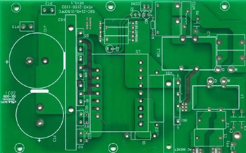
The metal surface treatment of metal contacts and terminals is mainly for loading and connecting various electronic components. Common metal surface treatment of circuit board is shown in Figure 1
At present, the most commonly used soldering tin is 63/37 eutectic tin lead. However, due to environmental factors, lead containing products will be banned in the future, so various alternatives have been proposed. At present, lead-free soldering solutions include Sn Ag, Sn Ag Cu, Sn Ag Bi, Sn Cu, etc. Although there are many kinds of lead-free soldering solutions, they are all solder pastes. It seems that materials are not a problem in assembly. However, in terms of metal surface treatment of circuit boards, it is impossible to find fully compatible products.
(1) HASL - Hot Air Solder Leveling
After the solder stop paint is applied on the circuit board, the copper surface exposed to the air must be protected. One method is to attach a layer of solder to the copper surface. As soldering tin is generally used for electronic welding, its melting point is below 200 ° C. If it is melted into a furnace, it can be directly coated with a layer of solder protective film on the copper surface by soaking. These solders are just the same as those used for future welding, which is conducive to the assembly of components. However, by soaking, the tin deposition on the circuit board surface will be too high and uncontrolled. Therefore, high pressure hot air is used to scrape off the excess tin on the surface and blow out the residual tin in the through-hole to protect the copper surface and the inner wall of the hole.
The general tin spraying process is: degreasing - micro etching - pickling - drying - flux coating - HAL - cooling - cleaning - drying
HASL is to immerse the circuit board in molten solder, and blow high-temperature and high-pressure air on the panel with the air knife when pulling out, so as to control the thickness of solder. Because it is very difficult to level the whole board surface with hot air in a short time, the installation of thinner copper pads may be problematic when assembling components. As the tin is not completely cooled and solidified at the moment of tin spraying, the horizontal placement will generally have a good thickness distribution. Of course, the tin thickness of horizontal tin spraying is different from that of vertical tin spraying, and the uniformity of horizontal tin spraying is slightly better than that of vertical tin spraying in general experience, but the maintenance of horizontal tin spraying machine is more troublesome. In the near future, due to the lead-free demand of environmental protection issues, there are doubts about whether the tin spraying process will continue to be used, and the selection of solder has become an urgent matter.
(2) Organic protective film (0SP) Note 113
It is another way of metal surface treatment to cover the copper surface not covered by the welding stop paint with heat resistant organic protective film, which is also called pre flux, because the following process is welding components. The fresh copper surface has solderability. If the fresh copper surface can be kept with organic precipitation layer, the subsequent solderability can be kept. In fact, not all organic protective films have soldering ability. Except for a few rosin series protective films, most protective films have only protective functions. Therefore, the protective film must be compatible with the flux during the subsequent welding. Generally speaking, if an organic protective film is used, the flux used for welding needs to be slightly more active. A stronger flux can decompose the organic film in a thermal environment and directly connect tin and copper substrate.
The current assembly often has more than one remelting process, so the organic film must pass a certain heat resistance test to be competent.
(3) Selective tin plating
In the process of making lines by line electroplating, solder can be directly plated on the line area as an etching barrier layer. After etching, the photoresist film is stripped, and then the second photoresist film selection is made to cover the solder area to be retained. Then, the uncovered area is removed with the stripping solution, and the area to be soldered is reserved for welding. This practice must be carried out when the line is electroplated. If the line is formed, it cannot be carried out if the wire is lost. Therefore, most of them still use the tin spraying process to make solder coating.
Most tin and lead fluoroborate electroplating systems are used for tin and lead electroplating, and some users use organic acid electroplating systems. The composition of the tin electroplated is about 60/40 tin to lead.
The circuit made for welding must control the precipitation amount on the copper pad, so the current density and distribution must be controlled, otherwise not only the thickness but also the composition will deviate.
(4) Nickel/Gold Plating
In some applications, multilayer circuit boards and high-density multiplayer boards may be mixed with bare crystal assembly and component assembly. Recently, due to the gradual growth of organic packaging boards, BGA, PGA, CSP and other packaging boards will have the demand for wire bonding. These boards that need bonding must be treated with full board nickel gold plating.
The common coating thickness is about 1-5 m for nickel, and about 0.05-0.75 m for gold. Nickel sulfamate bath is widely used because of low coating stress.
The gold plating system commonly used for gold plating fingers is not suitable for gold plating by wire striking. The plating solution with metal system additives will make the coating hard. Hard gold has good wear resistance in connector application, and soft gold is similar to pure gold, so it is more suitable for wiring. Because electroplating precipitation is used, the electroplating area must be connected with the electrode, and then cut off after electroplating. Due to the antenna effect of the residual wire in the circuit board, some manufacturers block the connection with a light barrier before electroplating, and strip the light barrier and etch the connector pins after electroplating. Therefore, there is a so-called Etch Back process, which is not the same thing as the early American military talk about Etch Back.
The production of chemical nickel/gold ^ 16 does not require the use of current, so there is no need for line connection. Therefore, the elasticity of circuit board production has been greatly improved. Most manufacturers carry out chemical nickel process The catalyst is similar to the chemical copper system. As the phosphate system reductant is used, the precipitated nickel will have phosphorus eutectoid, and the phosphorus content will affect the physical properties of the coating, so the eutectoid amount must be controlled.
Chemical gold precipitation is basically divided into replacement gold system and reducing gold system. Most of the current users are replaced chemical gold, which can produce thin coatings with a gold thickness of 0.05-0.1m or less. The application of thick coating is still suitable for reducing gold, and some applications reach 0.5m. When gold is replaced, pinholes will be formed due to the ion exchange with the nickel surface, but this phenomenon is less likely because the reducing gold is precipitated by catalyst. Most of the electroless gold plating solutions are cyano based systems. Because such substances may damage the organic layer of the solder stop paint, some manufacturers are working hard to develop gold sulfite systems
For the application of packaging board assembled with gold wire, high purity and thick gold ore layer will be required. For the product application mainly based on welding or aluminum wire, low gold plating thickness will be required.
III. Machining
In order to meet the final assembly requirements, the circuit board must be formed and machined. The high degree of freedom of SMT processing and PCBA processing can meet various requirements. In order to solve the problem of assembly efficiency, the assembly operation will first assemble many single circuit boards when they are integrated together. After the assembly test of the parts, the work of dividing the single piece shall be carried out. In order to make the subsequent segmentation easy, the circuit board is often processed with broken V-shaped groove, broken hole drilling, etc. to make the post assembly processing easy. For products with strict appearance requirements, the milling machine (Router) will be used for cutting, and the punching machine is also used for less strict products. At this stage, the assembly tool hole will be made at the same time, and some oversized non electroplating through holes can also be processed here. As for interface card products, chamfering will be carried out for smooth operation due to frequent plugging and unplugging
After the overall machining, there will be a lot of powder chips on the circuit board surface that must be removed. Therefore, the final cleaning action must be carried out to remove the cutting powder or the dirt during processing. After drying, the finished product will be the finished product after shipping inspection.


Just upload Gerber files, BOM files and design files, and the KINGFORD team will provide a complete quotation within 24h.