
Professional PCB manufacturing and assembly
Building 6, Zone 3, Yuekang Road,Bao'an District, Shenzhen, China
+86-13410863085Mon.-Sat.08:00-20:00

Bare copper design under board to board connector
Recently, our circuit board manufacturer found that a purchased module had a problem of poor function test. The problem was not 100%, but there were nearly 0.5~4% defects. At the beginning of the analysis, it was found that the contact was unstable, because this module used a board to board connector to connect externally. During the measurement, it was found that some PIN pins had a short circuit to ground, but sometimes the short circuit could not be measured, The response was sent to the supplier and the defective products were sent to the supplier for analysis, but the cause was never found.
After a lot of trouble, I simply disassembled the board to board connector for inspection. I wanted to say that the dead horse was a living horse doctor. After disassembling it, I found that this module had two bare copper areas on the board under its board to board connector, and the bare copper was just the place where the PIN pin ground short circuit occurred. I reported the problem to the supplier again, and invited the highest level of the company's procurement (Lao Mei spoke) to exert pressure, So the supplier (German manufacturer) cooperated with us to carry out urgent daily meeting tracking.
Finally, the supplier couldn't stand it, and probably found the problem. The supplier finally admitted that one of the board to board connectors it used might have a problem, and the problem might be caused by the large burr of the terminal section. Later, we blew down the connector of the module in question (a little ugly) and observed it under a microscope. It was found that there was burr, and the burr was really large. In addition to the pressure applied after the assembly of the board to board connector, the chance of the burr contacting the grounding bare copper area to form a short circuit should be very large.
The problem has been found, and the next problem is sorting and material replacement.
doubt:
Why should bare copper be designed under board to board connectors for circuit boards?
The answer is to prevent ESD. (Later, the bare copper was reduced to one piece, and it was found that the ability of ESD became worse.)
Why do not all board to board connectors have this problem?
Other connector suppliers do not make the cutting section of the terminal at the same place during mold design, so the place where the burrs are generated is different.
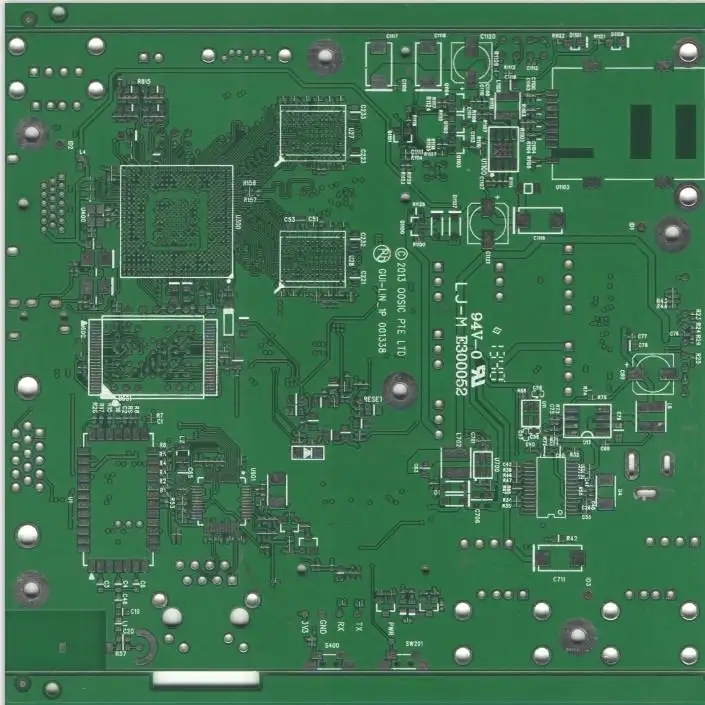
▼ After the board to board connector is damaged, it is found that the board below it has a bare copper grounding design.
▼ Remove all the board to board connectors. It is found that there are two square designs of bare copper under the board.
▼ After blowing off the board to board connector, it is found that the cutting section of its terminal has large burr.
▼ Compare the PCBA board to board connector with the wiring solder pad of the circuit board, and the place with burrs on the cutting section of the terminal just points to the bare copper area.


Just upload Gerber files, BOM files and design files, and the KINGFORD team will provide a complete quotation within 24h.