
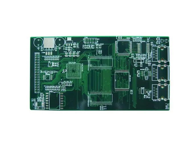
Professional PCB manufacturing and assembly
Building 6, Zone 3, Yuekang Road,Bao'an District, Shenzhen, China
+86-13410863085Mon.-Sat.08:00-20:00

Materials for high-density multilayer circuit boards
Multilayer circuit boards have always been manufactured by through hole electroplating. Since 1990, various layer adding technologies have been proposed, and many materials for layer adding process have been developed. If special manufacturing methods are not included, there are three general types of laminating materials, which are photosensitive resin, thermosetting resin, and resin coated copper foil. Other materials can also be incorporated into three types of base materials according to the operation mode. The second 70 is a comparison of some advantages and disadvantages of general high-density multilayer circuit boards. Due to the gradual popularization of high-density laminate, there are not only many manufacturers but also changing material characteristics, so it is not appropriate to introduce specific products. Moreover, for special suppliers and users, many evaluations will be different from the judgments in the table, so the contents in the table are only for reference
Each resin system will adjust its characteristics according to the requirements of the process, and its characteristics are composed of basic resin monomer (Monomer) to 51, hardener (Hardener) 52, stabilizer, additive, filler, etc. The demand of liquid resin is similar to that of solder stop paint ink, which is mainly beneficial to coating and conforms to the characteristics of the final product. Vacuum pressed film is similar to ordinary dry film, but the resin must have the characteristics of dielectric materials. Hot pressed materials shall have the characteristic reaction of traditional films.
A photosensitive dielectric material
This kind of material is mostly developed from a series of photosensitive solder stop paint products. Its micropore formation is completed by using negative film exposure. Because all micropores can be made at one time without pore density (via). Therefore, in the early stage of development of high-density laminate, it is very promising that chemical copper and electroplating copper must form a circuit connection after microporous processing. In order to improve the adhesion with chemical copper, the surface roughness must be made before chemical copper to improve the adhesion of copper. Since copper foil is not used, full plate electroplating total etching process or SAP Semi Additive Process will be used to make circuits.
Because the physical properties and photosensitivity of the photosensitive dielectric materials must be considered, it is difficult to control the formulation of the materials. This kind of resin has liquid ink and film forms. Liquid products can be coated by screen printing, curtain coating, roller coating, etc. Since the flatness is difficult to control, the material characteristics, pressing or coating machines, operating conditions, etc. used must be properly controlled and selected.
Although the production cost of resin film is high, it has great advantages in operation, thickness control and cleanliness, so some products are also made into film. As the film is to be pressed on the concave and convex surface, the vacuum film pressing machine is used for film pressing.
Optical pore forming technology is to transfer the image of the hole position with the negative film, and make small holes through UV sensitization, development and other procedures. Depending on the resin system used, the developer has two system products: alkaline aqueous solution and organic solvent. The environmental protection problem of the aqueous solution system is relatively small, while solvent based products are more troublesome. However, some products will still use solvent based design for the overall resin characteristics.
Second heat hardening resin material
This kind of resin will use carbon dioxide laser or UV laser for microporous processing, so the resin formulation does not need to consider the sensitivity. Relative resin use flexibility is wider, and the physical properties of the product are relatively easy to achieve. In general, the characteristics of this kind of resin system mainly focus on the absorption of laser light, fluorescence reflection characteristics, chemical resistance, coarsening applicability and other characteristics.
This kind of resin products include liquid ink and film. After coating or film pressing, laser drilling is carried out, and then interlayer conduction and circuit production are carried out by electroplating. As there is no surface copper, chemical copper treatment must be carried out as the seed layer for electroplating. In order to ensure the bonding force between copper and resin, the resin surface must be coarsened to obtain the anchor force. Generally, the tensile force that can be achieved is about 0.8? 1.2kg/cm。
The basic coating method of liquid resin is the same as that of photosensitive resin, and the film type material is also similar to that of photosensitive resin. Generally, the film thickness of high-density laminated circuit boards is 40? 80//m. As there is no copper sheet on the board, no matter it is photosensitive or heat hardening resin, it is conducive to the production of thin lines due to less etching.
Three resin copper sheet material, or gum copper sheet
This kind of material is mainly developed to conform to the traditional circuit board production mode, and the method is to coat the B-stage heat hardening resin on the roughened surface of the copper sheet. The thickness of copper sheet used is generally 12 # m or 18//m, but ultra-thin copper sheet will be used for special purposes. The thickness of the resin must be determined according to the demand for filling amount, and generally the thickness after pressing is taken as the index.
Due to the copper sheet pressing process, the bonding force comes from the bonding force between resin melting and copper sheet. The copper sheet tension is relatively stable, similar to that of traditional circuit boards. The use of hot pressing technology and traditional stack method has better compatibility in the use of tools and operations. The reason why it is widely used is that the manufacturing process is easy to import. Many manufacturers have put it into production.
At the initial stage of development of high-density laminate, such materials will open a copper window (Conformal Mask) on the copper foil by image transfer and etching, so this process is called Conformal Mask. A few years later, due to the progress of laser technology and the gradual maturity of process technology, some processing also began to explore the direct laser processing mode, so this process is called LDD Laser Direct Drill Note 53. Due to the shielding of copper, the whole board surface after adding layers is covered by copper foil. How to make reference identification is a problem that must be faced. This is the so-called tool system collocation, which must be taken into consideration during manufacturing and design.
Such materials still have to rely on etching when making circuits, and the etching amount is much larger than that of circuit boards without copper skin, so it is not conducive to the control of circuit accuracy. This is why many copper skin manufacturers have invested in the development and production of thin copper skin recently.
IV. Other types of materials
Of course, the materials used for high-density laminated circuit boards are not only limited to those mentioned above, but also products of different forms are being used or developed. For example, some products are not satisfied with the structure of unreinforced fibers, but the addition of fibers is not conducive to processing. Therefore, in order to improve the physical properties of circuit boards, special flat glass fiber materials will be used to make laser processing layers. At this time, not only the pressing process and expansion and contraction design must be reconsidered, but also the laser processing conditions must be readjusted.
As for the quite well-known ALIVH process, the film is made of Aramid fiber non-woven fabric impregnated resin, so the material is easier to be laser processed.
B2IT uses silver paste to form bumps to penetrate the film, and then uses copper sheet bonding by pressing. Therefore, the silver glue used is special, and the selection of film is less limited.
Goretex Company in the United States uses PTFE fiber to make fibrous film. Because PTFE can reduce the dielectric constant, it is conducive to high-speed transmission of products.
V. High frequency material trend
From the evolution of personal computers, it can be seen that the speed of CPU generation alternation is getting faster and faster, and consumers are overwhelmed. Of course, this is a good thing for the public. However, it is a further challenge to the production of PCB. Because of high frequency, lower Dk and Df values of the substrate are required.


Just upload Gerber files, BOM files and design files, and the KINGFORD team will provide a complete quotation within 24h.