
Professional PCB manufacturing and assembly
Building 6, Zone 3, Yuekang Road,Bao'an District, Shenzhen, China
+86-13410863085Mon.-Sat.08:00-20:00

The method and step flow of self-made PCB
Corrosion method of circuit board:
Corrosion solution is generally prepared with ferric chloride and water. Ferric chloride is an earthy yellow solid and easy to absorb water in the air, so it should be sealed for storage. When preparing ferric chloride solution, generally 40% ferric chloride and 60% water are used. Of course, more ferric chloride is used, or warm water (not hot water, to prevent paint falling off) can make the reaction faster. Note that ferric chloride has certain corrosivity, It is better not to get it on the skin and clothes (it is difficult to wash: - (The reaction container is a cheap plastic basin, which is good for holding the circuit board. Corrosion starts from the edge. When the copper foil without paint is corroded, the circuit board should be taken out in time to prevent the useful circuit from being corroded after the paint falls off. At this time, wash it with clean water, and scrape the paint with bamboo chips and other things (at this time, the paint comes out of the liquid, which is easier to remove). If it is not easy to scratch, just rinse it with hot water. Then it is wiped dry and polished with sandpaper to reveal shiny copper foil. A printed circuit board is ready. In order to preserve the achievements, Bitbaby usually uses rosin solution to coat the polished circuit board once, which can not only aid welding, but also prevent oxidation. The circuit board is the carrier of electronic circuits. Any circuit design needs to be installed on a circuit board to realize its function. And processing circuit boards is the most headache for amateur electronics enthusiasts. It often takes half a day to design circuits, but it takes several days to process circuit boards. Even some very good circuit design ideas, but because it takes too much time to process the circuit board, they give up the experiment and cannot continue to realize. The stationmaster began to do circuit experiments more than 20 years ago, and the most brilliant thing is to make circuit boards. It can be said that he has tried every means: paint, paraffin, carbon paper, carving knife, even nail polish, eyebrow pencil and other things used by MM, but still can not achieve the goal of making experimental circuit boards efficiently and high-quality.
Later, when I went to the company to engage in professional design and development, I learned that professional engineers did not know there was such a difficulty. They use CAD to design the drawings, print them out and hand them to the PCB processing plant. After a few days, they can get several processed PCB templates. Install the parts, debug and modify them before printing, and then send them to the PCB processing plant for processing. Repeat several times, and the circuit is ready. They do not need to consider all kinds of tedious technological processes and production costs in the process of processing circuit boards. However, the reason why PCB manufacturers have to take the trouble to repeatedly process experimental circuit boards for these companies for free is certainly not to "carry forward the spirit of Lei Feng". It is obvious that these processing costs are to be apportioned to the costs of future mass production.
If you are a small unknown company or an individual, the cost of processing may be hundreds of yuan. Therefore, how to process experimental circuit boards with simplicity, rapidity, low cost and high quality is a subject worthy of study. Now there are also many new good methods, such as: thermal transfer printing, precoating photosensitive copper-clad, hot-melt plastic film, etc. This website will collect the methods and experiences in this field, compile them into articles, and publish them on this website in succession. Fans, manufacturers, material and equipment suppliers are also welcome to cooperate, or write articles, or provide your products, or cooperate to promote.
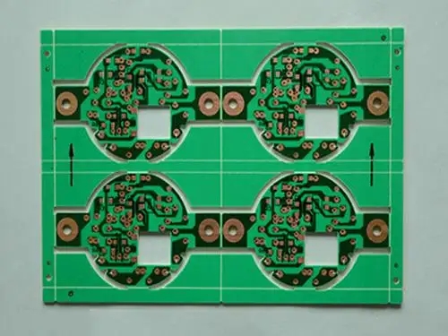
As stated in the foreword, the circuit board is the carrier of the circuit, which is commonly referred to as "printed circuit board". The regular production of printed circuit boards is naturally related to printing, and the screen printing process is usually adopted. The basic process is as follows: layout design → tracing → drying the board (making the printing plate) → printing → chemical corrosion → cleaning and surface treatment → printing soldering, marking, solder mask and other layers → cutting, punching and other mechanical processing → finished circuit boards
For more detailed operation steps, please refer to the article "Making Circuit Boards and Instrument Signage Panels by Screen Printing" collected on this site (in the column of "Practice Basis").
Under amateur conditions, the process of "printing soldering, identification, solder mask and other layers" can be omitted, and the difficulty lies in plate making and printing. Since only a few (one or several) circuit boards need to be produced, it is obviously uneconomical to adopt normal plate making and printing processes, so there are various non printing or sub printing production methods.
1. Carving method
This method is the most direct. Use carbon paper to copy the designed copper foil pattern to the copper foil surface of the copper clad laminate. Use a special carving tool made of a hacksaw blade to carve along the edge of the copper foil pattern directly on the copper clad laminate, cutting as far as possible to the depth, then tear off the unwanted copper foil outside the pattern, and then punch the jack of the component. The key to this method is: the intensity of portrayal should be sufficient; The excess copper foil shall be removed from the edge of the board. If the operation is good, it can be removed gradually in pieces. The nail clipper can be used to complete this step. Some small circuit experimental plates are suitable for making with this method.
2. Manual delineation
It is to use a pen to directly draw the printed graphics on the CCL, and then conduct chemical corrosion and other steps. This method seems simple, but it is not easy to operate! Today's electronic components are small in size, with smaller pin spacing (millimeter scale). The copper foil wiring is also small, and the lines drawn on them are difficult to modify. It depends on your pen work to draw such a board. The experience is that the selection of "pigments" and brushes is crucial. I used to use red nail polish in a medical syringe to paint a circuit board. The effect was good, but the tip of the needle should be properly processed; It was also introduced to use paint chips dissolved in anhydrous alcohol to draw with a pen. The specific methods are as follows:
Dissolve one piece of paint (shellac, available in chemical raw material stores) in three parts of anhydrous alcohol, and stir it properly. After it is completely dissolved, drop a few drops of medical violet (gentian violet) to make it appear a certain color. After stirring evenly, it can be used as protective paint to paint circuit boards. First polish the copper-clad plate with fine sandpaper, and then use the duckbill pen (or the ink duckbill pen used to draw figures on the compass) in the drawing instrument to paint. The duckbill pen has a nut to adjust the stroke thickness. The stroke thickness can be adjusted, and the ruler and triangular ruler can be used to draw very thin straight lines, and the lines described are smooth, uniform, without edge serrations, giving a smooth and fluent feeling; At the same time, you can also write lines described by Chinese characters, English, Pinyin or symbols in the spare place of the circuit board. If you soak around, the concentration is too small, you can add a little paint chip; If the pen cannot be drawn, it is too thick, and a few drops of absolute alcohol are needed. It doesn't matter if the description is wrong. Just use a small stick (matchstick) to make a small cotton swab, dip it in a little absolute alcohol, and then easily wipe it off, and then paint again. Once the circuit board diagram is drawn, it can be corroded in ferric chloride solution. After the circuit board is corroded, it is also very convenient to remove the paint. Use cotton balls dipped with absolute alcohol to wipe off the protective paint. After drying slightly, it can be used with pine perfume.
As the alcohol volatilizes quickly, the prepared protective paint should be sealed and stored in a small bottle (such as an ink bottle). Don't forget to cover the bottle after use. If the concentration is thickened in the next use, just add an appropriate amount of anhydrous alcohol.
3. Posting method
There is a "standard pre cutting symbol and tape" available in electronic stores. Common specifications of pre cutting symbols include D373 (0D-2.79, ID-0.79), D266 (0D-2.00, ID-0.80), D237 (OD-3.50, ID-1.50), etc. It is better to buy paper based materials (black) and plastic based materials (red). Common specifications of tape include 0.3, 0.9, 1.8, 2.3, 3.7, etc. The unit is mm. According to the circuit design layout, the corresponding symbols and tapes can be selected and pasted on the copper foil surface of the copper clad plate. Use a soft hammer, such as smooth rubber and plastic, to knock the decal to fully adhere to the copper foil. Focus on striking the turning and overlapping points of the line. In cold weather, it is better to heat the surface with a heater to strengthen the adhesion effect. After being posted, the corrosion process can be carried out.
4. Mimeography
Put the wax paper on the steel plate, use a pen to engrave the circuit diagram on the wax paper in 1:1, and cut the circuit diagram engraved on the wax paper according to the size of the circuit board, and put the cut wax paper on the printed copper plate. Take a small amount of paint and talcum powder, mix them into a thin and thick printing material, dip the printing material with a brush, evenly smear it on the wax paper, repeat several times, and the printed board can be printed with the circuit. The stereotype can be used repeatedly and is suitable for small batch production. Tips: Photoelectric copying machine can be automatically engraved into 1:1 size wax paper according to design drawings.
5. Hot melt plastic film plate making method: This method is collected from online articles (by NewBlue), and its feasibility has not been verified for reference.
① Print the circuit board diagram on 80g copy paper at a scale of 1:1 on the printer. Manual drawing is OK, but the bottom paper should be flat.
② Find a fax machine, take out the fax paper in the machine and replace it with hot melt plastic film (it is said that it can be bought, please contact the stationmaster who has this product). Put the circuit diagram into the entrance of the fax machine, and use the copy key of the fax machine to copy the circuit diagram on the hot melt plastic film. At this time, the "printed manuscript" of the PCB is ready.
③ Use double-sided adhesive tape to paste the plastic film of the prepared drawing on the copper clad plate. Attention shall be paid to the flatness without wrinkles, and the adhesive tape shall not cover the melting part, otherwise the production effect of the circuit board will be affected.
④ Use a paint brush to evenly brush the paint on the plastic film. Note: do not brush repeatedly, but brush in one direction in turn, otherwise the plastic film will wrinkle together and the lines on the copper plate will overlap. Remove the plastic film carefully after the circuit diagram is completely brushed. At this time, a printed circuit board is printed. After drying, it can be corroded. If you want to print more than one piece, you can make a wooden frame a little larger than the circuit board, lay the wire mesh on the wooden frame evenly and fix it. Then use double-sided adhesive tape to paste the plastic film with fixed shadow under the screen. Put the copper plate on the table, close the wire mesh frame (the printed drawing and the copper plate should be aligned left and right), brush the paint in one direction with a paint brush, and remove the wire mesh frame. The printed circuit board is ready. In case of defects, paint and bamboo chips can be used for modification. Attention shall be paid to the above process. When painting, the hand force shall be appropriate. If the paint film is too thick, the lines will run away from lace, and if the paint is too light, the lines will break. The plastic film must face up.
6. Use pre coated photosensitive copperplate
A special copper clad plate is used. A layer of photosensitive material is pre coated on the surface of the copper platinum layer, so it is called "pre coated photosensitive copper clad plate", also called "photosensitive plate". The production method is as follows:
① Production of single panel: print 1:1 black and white 720dpi drawings (component surface) with special inkjet paper from the PCB drawing drawn by the computer. It is also possible to output drawings with laser printer. Take a photosensitive plate with the size of the drawing and tear off the protective film. Press the drawing and the photosensitive PCB with glass plate or plastic transparent plate, and expose them to the sun for 5-10 minutes. Use the attached developing agent 1:20 to prepare water for development. When the exposed part (unnecessary copper coating) is completely exposed, rinse it with water, and then it can be corroded with ferric chloride. After skilled operation, the routing with an accuracy of 0.1mm can be made!
② Fabrication of double-sided circuit board: refer to the single panel for the steps. The double-sided circuit board is mainly positioned accurately on both sides. Both sides can be exposed separately, but the time shall be consistent. One side shall be protected with black paper when exposed. This method is the simplest and practical method in principle, but because of the high price of the commercially available "precoated photosensitive copper clad plate", it is not easy to buy. So this method is not known by most amateurs. Welcome to contact our website for cooperation and promotion.
7. Heat transfer printing
Use a laser printer to print the designed PCB copper platinum graphics on the thermal transfer paper, and then attach the thermal transfer paper to the copper platinum surface of the copper clad plate. Heat it at an appropriate temperature. The graphics originally printed on the transfer paper (actually carbon powder) will be heated and melted, and transferred to the copper platinum surface to form a corrosion protection layer. This method is simpler than the conventional plate making and printing method, and now most of the circuits are designed using computer CAD, laser printers are also quite popular, and this process is relatively easy to achieve.


Just upload Gerber files, BOM files and design files, and the KINGFORD team will provide a complete quotation within 24h.